gokul/flex-led-wristband
A flexible, rechargeable touch wristband PCB with MCP73831 Li-ion charging, switched 3.0 V regulation, ATtiny402 control, TTP223 capacitive touch sensing, and six charlieplexed red LEDs plus power/charge indicators.
- Version
- 0.0.3
- License
- unset
- Stars
- 0
FABRICATION.txt
FLEX LED WRISTBAND — JLCPCB PROTOTYPE FABRICATION SPECIFICATION — REV 0.0.3

BOARD
Two copper layers on polyimide flex, nominal finished thickness 0.12 mm, 0.5 oz (nominal 18 um) electro-deposited copper per layer, ENIG exposed finish. Use JLCPCB's standard 2-layer flex process; CAM must confirm the actual dielectric/adhesive/coverlay stack. This is flex with bonded stiffeners, not integrated rigid-flex. No impedance requirement. Do not substitute rigid FR4 for the flex substrate.

OUTLINE AND STIFFENERS
90 x 32 mm maximum, 10 mm wings, 1 mm nominal corner radii approximated with short chords in Gerber. Edge_Cuts.gbr is authoritative. Centre bottom FR4 stiffener 30 x 30 mm, 0.40 mm plus nominal 0.05 mm adhesive (fr4b_0.4.gbr). Six bottom PI stiffeners, each 6 x 8 mm, 0.20 mm plus nominal 0.05 mm adhesive (pib_0.2.gbr), centred at x = -40,-30,-20,20,30,40 mm, y = 0. Board-centred coordinates, +Y up. Do not scale or mirror stiffener artwork independently. Confirm both materials and adhesive stack in CAM.

COPPER / DRILLS
Minimum track width and clearance 0.20 mm. Vias 0.30 mm finished hole / 0.60 mm pad; tent with coverlay both sides. Two switch locating holes: NPTH 0.90 mm, centres (-3.4,11) and (3.4,11). All via pads contained within reinforced regions. No bottom routing in designated unsupported wing spans or beneath the touch electrode. External contacts: copper 2.50 x 3.10 mm, opening 1.80 x 2.40 mm. Preserve 0.35 mm coverlay overlap on each edge for anchoring.

COVERLAY / PASTE
Use F_Mask/B_Mask as coverlay openings; preserve grouped rectangular openings for each pin row of U2/U3. Do not split into individual openings or automatically expand wire-contact openings. Measured minimum web in dist/manufacturing-checks.json is >=0.50 mm. Touch electrode is covered; no paste on it or wire/programming contacts. Vias covered. Request production-file confirmation before manufacture, especially mask-defined contact openings, stiffener alignment and layer stack. Standard rigid-board solder-mask processing is not assumed.

MECHANICAL USE
Gentle static wrist curvature only; nominal intended bend radius >=12 mm, pending JLCPCB stackup approval. Bend only in unsupported spans, never at a component, via or stiffener boundary. No sharp folding. Strap carries tension and battery weight. Battery remains flat in a rigid insulated enclosure; wires need strain relief. The live quote form disables rolled-annealed copper at 0.12 mm; this release specifies electro-deposited copper. Continuous dynamic flex is not qualified.

ASSEMBLY
25 top-side SMT parts. Use assembly-bom.csv, assembly-placement.csv, assembly-orientation.csv and assembly.svg together. Origin board centre; +Y up; millimetres. SW1 physical body centre is (0,11), not its pad-bounding-box centre. Rotations are design angles, not certified JLC supplier-library mapping: verify IC pin 1 and LED cathodes in assembly preview. LEDs have cathode on circuit pin2; internal pin1 numbering is not a vendor cathode convention. SW1 pin2 common, pin3 regulator input; ON=2-3, OFF=1-2. Switch pad width follows C&K's 1.20 mm drawing. JLCPCB must confirm sourcing, rotations and flex assembly carrier/fixture before PCBA. Substitutions require electrical and footprint review.

EXTERNAL POWER
Protected 1S LiPo, 3.7 V nominal / 4.2 V maximum; cell must permit >=50 mA charging. No onboard cell protection, temperature sensing or load sharing. Use regulated 5 V charging fixture, correct polarity. Switch OFF while charging; charge off wrist. Target-powered 3 V UPDI; do not backfeed VCC from another supply.

RELEASE LIMIT
Design-level electrical/geometry checks are not JLCPCB CAM approval or tested hardware. Before wearing: charger termination, regulation, LED scanning, touch sensitivity, battery cutoff, insulation, strain relief and flex durability must pass prototype checks. Firmware is not included.

JLCPCB references reviewed 22 October 2026:
https://jlcpcb.com/capabilities/flex-pcb-capabilities/
https://jlcpcb.com/help/article/fpc-stiffener-emi-guide
https://jlcpcb.com/blog/fpc-parameters-optimal-performance
https://jlcpcb.com/blog/must-know-flex-pcb-tips-45
https://jlcpcb.com/help/article/how-to-order-boards-with-solder-mask-defined-pads
https://jlcpcb.com/help/article/pcb-assembly-fixtures
Related Packages
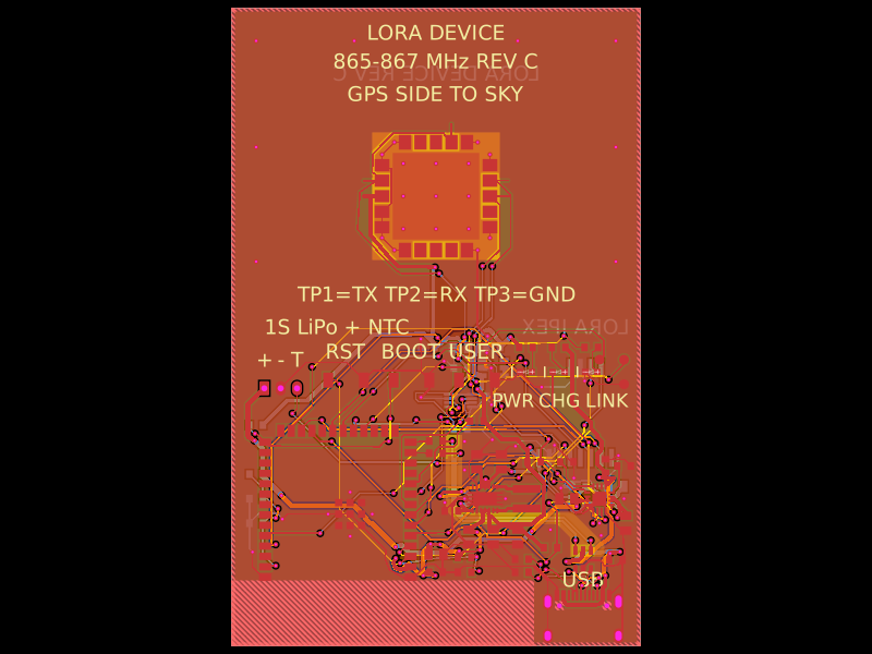 More from this authorgokul/lora-deviceA compact LoRa/GNSS device PCB integrating an SX1262 radio, GNSS module, USB/UART interface, 1.5 µH inductor, LiPo battery connector with NTC, and supporting passives.
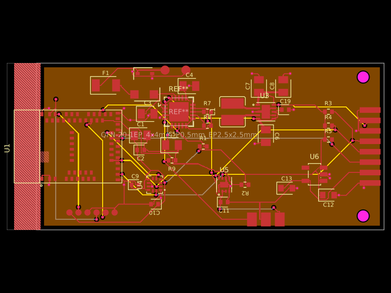 Similar packagemohan-bee/fitness-bandA 4-layer BLE wearable mainboard with Li-ion charging/protection, 3.3/1.8 V power regulation, motion and battery sensing, plus a folded 2-layer flex sensor board carrying MAX30102 optical and TMP117 temperature sensors.
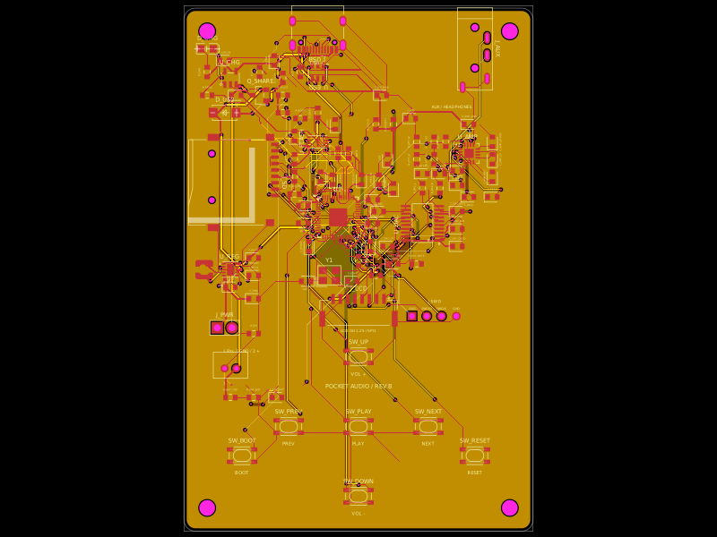 Discover something newDevesh36/pocket-audio-playerA portable, rechargeable microSD audio player built around an RP2040, SPI flash, USB‑C charging/power management, LCD/button controls, PCM5102A I²S DAC, and TPA6132A headphone amplifier in a 3D‑printed enclosure.