gokul/display
This schematic represents a compact electronic clock module integrating microchips, a 5V power supply, multiple 7-segment displays with driver ICs, reset/debounce circuitry, and supporting passive components on a printed circuit board (PCB).
- Version
- 0.1.4
- License
- unset
- Stars
- 0
index.tsx
PCB
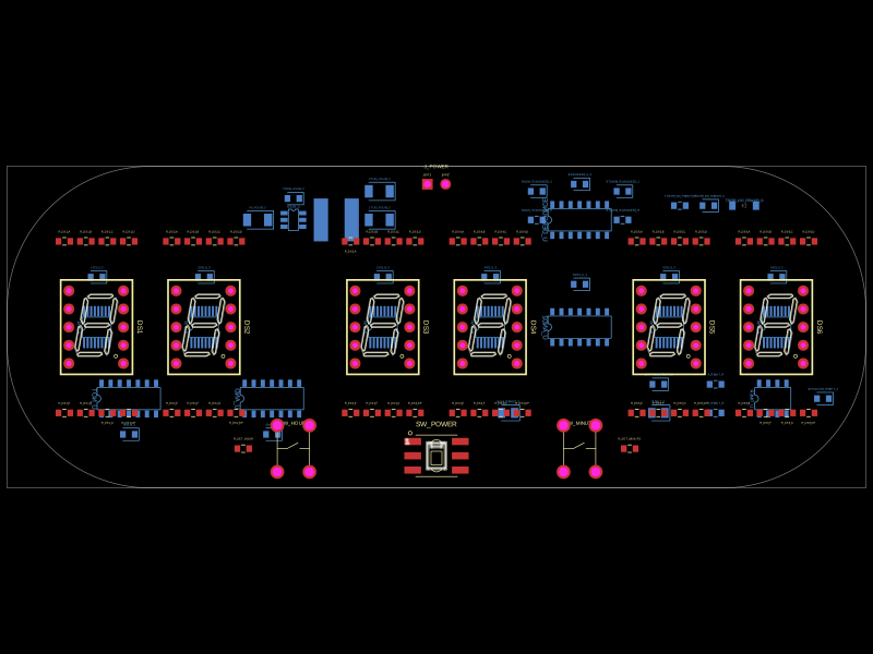
Schematic

import { FJ3191AH } from "./imports/c44296"
import { YTSPS_22E58LM } from "./imports/c2941005"


const unusedSegments = [
  "g",
  "f",
  "e",
  "d",
  "dp",
  "c",
  "b",
  "a",
]

const cd4093PinLabels = {
  pin1: ["A1"],
  pin2: ["B1"],
  pin3: ["Y1"],
  pin4: ["Y2"],
  pin5: ["B2"],
  pin6: ["A2"],
  pin7: ["VSS"],
  pin8: ["A3"],
  pin9: ["B3"],
  pin10: ["Y3"],
  pin11: ["Y4"],
  pin12: ["B4"],
  pin13: ["A4"],
  pin14: ["VDD"],
} as const

const timerPinLabels = {
  pin1: ["GND"],
  pin2: ["TRIGGER"],
  pin3: ["OUTPUT"],
  pin4: ["RESET"],
  pin5: ["CONTROL"],
  pin6: ["THRESHOLD"],
  pin7: ["DISCHARGE"],
  pin8: ["VDD"],
} as const

const cd4081PinLabels = {
  pin1: ["A1"],
  pin2: ["B1"],
  pin3: ["Y1"],
  pin4: ["Y2"],
  pin5: ["A2"],
  pin6: ["B2"],
  pin7: ["VSS"],
  pin8: ["A3"],
  pin9: ["B3"],
  pin10: ["Y3"],
  pin11: ["Y4"],
  pin12: ["A4"],
  pin13: ["B4"],
  pin14: ["VDD"],
} as const

const cd4069PinLabels = {
  pin1: ["A1"],
  pin2: ["Y1"],
  pin3: ["A2"],
  pin4: ["Y2"],
  pin5: ["A3"],
  pin6: ["Y3"],
  pin7: ["VSS"],
  pin8: ["Y4"],
  pin9: ["A4"],
  pin10: ["Y5"],
  pin11: ["A5"],
  pin12: ["Y6"],
  pin13: ["A6"],
  pin14: ["VDD"],
} as const

const cd4026PinLabels = {
  pin1: ["CLOCK"],
  pin2: ["CLOCK_INHIBIT"],
  pin3: ["DISPLAY_ENABLE_IN"],
  pin4: ["DISPLAY_ENABLE_OUT"],
  pin5: ["CARRY_OUT"],
  pin6: ["F"],
  pin7: ["G"],
  pin8: ["VSS"],
  pin9: ["D"],
  pin10: ["A"],
  pin11: ["E"],
  pin12: ["B"],
  pin13: ["C"],
  pin14: ["UNGATED_C"],
  pin15: ["RESET"],
  pin16: ["VDD"],
} as const

export default function DisplayBoard() {
  return (
    <board width="120mm" height="45mm" borderRadius="20mm">

  {/* 555 clock generator*/}

<chip
  name="U_TIMER"
  manufacturerPartNumber="TLC555IDR"
  footprint="soic8"
  pinLabels={timerPinLabels}
  pcbX={47}
  pcbY={-10}
  pcbRotation="90deg"
  layer="bottom"
  connections={{
    VDD: "net.V5",
    GND: "net.GND",
    RESET: "net.V5",
    OUTPUT: "net.CLOCK_1HZ",
    TRIGGER: "net.TIMER_RC",
    THRESHOLD: "net.TIMER_RC",
    DISCHARGE: "net.TIMER_DISCHARGE",
    CONTROL: "net.TIMER_CONTROL",
  }}
/>

<resistor
  name="R_TIMER_A"
  resistance="4.7kohm"
  footprint="0603"
  pcbX={39}
  pcbY={-8}
  layer="bottom"
  connections={{
    pin1: "net.V5",
    pin2: "net.TIMER_DISCHARGE",
  }}
/>

<resistor
  name="R_TIMER_B"
  resistance="68kohm"
  footprint="0603"
  pcbX={39}
  pcbY={-12}
  layer="bottom"
  connections={{
    pin1: "net.TIMER_DISCHARGE",
    pin2: "net.TIMER_RC",
  }}
/>

<capacitor
  name="C_TIMER"
  capacitance="10uF"
  footprint="0805"
  pcbX={31}
  pcbY={-12}
  layer="bottom"
  connections={{
    pin1: "net.TIMER_RC",
    pin2: "net.GND",
  }}
/>

<capacitor
  name="C_TIMER_CONTROL"
  capacitance="10nF"
  footprint="0603"
  pcbX={31}
  pcbY={-8}
  layer="bottom"
  connections={{
    pin1: "net.TIMER_CONTROL",
    pin2: "net.GND",
  }}
/>

<capacitor
  name="C_TIMER_DECOUPLE"
  capacitance="100nF"
  footprint="0603"
  pcbX={54}
  pcbY={-10}
  layer="bottom"
  connections={{
    pin1: "net.V5",
    pin2: "net.GND",
  }}
/>


  {/* 555 clock generator ends*/}
  {/* and gate ic*/}

  <chip
  name="U_AND"
  manufacturerPartNumber="CD4081BM96"
  footprint="soic14"
  pinLabels={cd4081PinLabels}
  pcbX={-23}
  pcbY={-10}
  pcbRotation="90deg"
  layer="bottom"
  noConnect={[
    "A1",
    "B1",
    "Y1",
    "A2",
    "B2",
    "Y2",
    "A3",
    "B3",
    "Y3",
    "A4",
    "B4",
    "Y4",
  ]}
  connections={{
    VDD: "net.V5",
    VSS: "net.GND",
  }}
/>

<capacitor
  name="C_U_AND"
  capacitance="100nF"
  footprint="0603"
  pcbX={-23}
  pcbY={-15}
  layer="bottom"
  connections={{
    pin1: "net.V5",
    pin2: "net.GND",
  }}
/>

{/* and gate ends*/}
{/* inverter ic starts*/}
<chip
  name="U_NOT"
  manufacturerPartNumber="CD4069UBM96"
  footprint="soic14"
  pinLabels={cd4069PinLabels}
  pcbX={-43}
  pcbY={-10}
  pcbRotation="90deg"
  layer="bottom"
  noConnect={[
    "A1",
    "Y1",
    "A2",
    "Y2",
    "A3",
    "Y3",
    "A4",
    "Y4",
    "A5",
    "Y5",
    "A6",
    "Y6",
  ]}
  connections={{
    VDD: "net.V5",
    VSS: "net.GND",
  }}
/>

<capacitor
  name="C_U_NOT"
  capacitance="100nF"
  footprint="0603"
  pcbX={-43}
  pcbY={-15}
  layer="bottom"
  connections={{
    pin1: "net.V5",
    pin2: "net.GND",
  }}
/>

{/* Main board supply filtering */}
<capacitor
  name="C_POWER_BULK"
  capacitance="10uF"
  footprint="0805"
  pcbX={10}
  pcbY={-12}
  layer="bottom"
  connections={{
    pin1: "net.V5",
    pin2: "net.GND",
  }}
/>

{/* inverter ic ends*/}


    {/*diplay 1 starts*/}


      <FJ3191AH
        name="DS1"
        pcbX={-47.5}
        pcbY={0}
        pcbRotation="270deg"
        connections={{
          GND1: "net.GND",
          GND2: "net.GND",
        }}
      />

      {/*resistor sets*/}
      {/*top row*/}

      <resistor
  name="R_DS1_A"
  resistance="220ohm"
  footprint="0603"
  pcbX={-52}
  pcbY={12}
/>

<resistor
  name="R_DS1_B"
  resistance="220ohm"
  footprint="0603"
  pcbX={-49}
  pcbY={12}
/>

<resistor
  name="R_DS1_C"
  resistance="220ohm"
  footprint="0603"
  pcbX={-46}
  pcbY={12}
/>

 <resistor
  name="R_DS1_D"
  resistance="220ohm"
  footprint="0603"
  pcbX={-43}
  pcbY={12}
/>

      {/*bottom row*/}

<resistor
  name="R_DS1_E"
  resistance="220ohm"
  footprint="0603"
  pcbX={-52}
  pcbY={-12}
/>

      <resistor
  name="R_DS1_F"
  resistance="220ohm"
  footprint="0603"
  pcbX={-49}
  pcbY={-12}

/>

<resistor
  name="R_DS1_G"
  resistance="220ohm"
  footprint="0603"
  pcbX={-46}
  pcbY={-12}

/>

<resistor
  name="R_DS1_DP"
  resistance="220ohm"
  footprint="0603"
  pcbX={-43}
  pcbY={-12}

/>

<chip
  name="U_DS1"
  manufacturerPartNumber="CD4026BPWR"
  footprint="tssop16"
  pinLabels={cd4026PinLabels}
  pcbX={-47.5}
  pcbY={0}
  pcbRotation="90deg"
  layer="bottom"
/>
<capacitor
  name="C_U_DS1"
  capacitance="100nF"
  footprint="0603"
  pcbX={-47.5}
  pcbY={7}
  layer="bottom"
/>

      {/*diplay 1 ends*/}

      {/*diplay 2 starts*/}

      <FJ3191AH
        name="DS2"
        pcbX={-32.5}
        pcbY={0}
        pcbRotation="270deg"
        connections={{
          GND1: "net.GND",
          GND2: "net.GND",
        }}
      />

      {/*resistor sets*/}
      {/*top row*/}
      <resistor
  name="R_DS2_A"
  resistance="220ohm"
  footprint="0603"
  pcbX={-37}
  pcbY={12}
/>

<resistor
  name="R_DS2_B"
  resistance="220ohm"
  footprint="0603"
  pcbX={-34}
  pcbY={12}
/>

<resistor
  name="R_DS2_C"
  resistance="220ohm"
  footprint="0603"
  pcbX={-31}
  pcbY={12}
/>

<resistor
  name="R_DS2_D"
  resistance="220ohm"
  footprint="0603"
  pcbX={-28}
  pcbY={12}
/>

{/*bottom row*/}
<resistor
  name="R_DS2_E"
  resistance="220ohm"
  footprint="0603"
  pcbX={-37}
  pcbY={-12}
/>

<resistor
  name="R_DS2_F"
  resistance="220ohm"
  footprint="0603"
  pcbX={-34}
  pcbY={-12}
/>

<resistor
  name="R_DS2_G"
  resistance="220ohm"
  footprint="0603"
  pcbX={-31}
  pcbY={-12}
/>

<resistor
  name="R_DS2_DP"
  resistance="220ohm"
  footprint="0603"
  pcbX={-28}
  pcbY={-12}
/>

<chip
  name="U_DS2"
  manufacturerPartNumber="CD4026BPWR"
  footprint="tssop16"
  pinLabels={cd4026PinLabels}
  pcbX={-32.5}
  pcbY={0}
  pcbRotation="90deg"
  layer="bottom"
/>


<capacitor
  name="C_U_DS2"
  capacitance="100nF"
  footprint="0603"
  pcbX={-32.5}
  pcbY={7}
  layer="bottom"
  connections={{
    pin1: "net.V5",
    pin2: "net.GND",
  }}
/>

      {/*diplay 2 ends*/}

      {/*diplay 3 starts*/}

      <FJ3191AH
        name="DS3"
        pcbX={-7.5}
        pcbY={0}
        pcbRotation="270deg"
        connections={{
          GND1: "net.GND",
          GND2: "net.GND",
        }}
      />

      {/*resistor sets*/}
      {/*top row*/}
      <resistor
  name="R_DS3_A"
  resistance="220ohm"
  footprint="0603"
  pcbX={-12}
  pcbY={12}
/>

<resistor
  name="R_DS3_B"
  resistance="220ohm"
  footprint="0603"
  pcbX={-9}
  pcbY={12}
/>

<resistor
  name="R_DS3_C"
  resistance="220ohm"
  footprint="0603"
  pcbX={-6}
  pcbY={12}
/>

<resistor
  name="R_DS3_D"
  resistance="220ohm"
  footprint="0603"
  pcbX={-3}
  pcbY={12}
/>

{/*bottom row*/}
<resistor
  name="R_DS3_E"
  resistance="220ohm"
  footprint="0603"
  pcbX={-12}
  pcbY={-12}
/>

<resistor
  name="R_DS3_F"
  resistance="220ohm"
  footprint="0603"
  pcbX={-9}
  pcbY={-12}
/>

<resistor
  name="R_DS3_G"
  resistance="220ohm"
  footprint="0603"
  pcbX={-6}
  pcbY={-12}
/>

<resistor
  name="R_DS3_DP"
  resistance="220ohm"
  footprint="0603"
  pcbX={-3}
  pcbY={-12}
/>

<chip
  name="U_DS3"
  manufacturerPartNumber="CD4026BPWR"
  footprint="tssop16"
  pinLabels={cd4026PinLabels}
  pcbX={-7.5}
  pcbY={0}
  pcbRotation="90deg"
  layer="bottom"
/>

<capacitor
  name="C_U_DS3"
  capacitance="100nF"
  footprint="0603"
  pcbX={-7.5}
  pcbY={7}
  layer="bottom"
/>

      {/*diplay 3 ends*/}

      {/*diplay 4 starts*/}

      <FJ3191AH
        name="DS4"
        pcbX={7.5}
        pcbY={0}
        pcbRotation="270deg"
        connections={{
          GND1: "net.GND",
          GND2: "net.GND",
        }}
      />

      {/*resistor sets*/}
      {/*top row*/}
<resistor
  name="R_DS4_A"
  resistance="220ohm"
  footprint="0603"
  pcbX={3}
  pcbY={12}
/>

<resistor
  name="R_DS4_B"
  resistance="220ohm"
  footprint="0603"
  pcbX={6}
  pcbY={12}
/>

<resistor
  name="R_DS4_C"
  resistance="220ohm"
  footprint="0603"
  pcbX={9}
  pcbY={12}
/>

<resistor
  name="R_DS4_D"
  resistance="220ohm"
  footprint="0603"
  pcbX={12}
  pcbY={12}
/>
  {/*bottom row*/}
<resistor
  name="R_DS4_E"
  resistance="220ohm"
  footprint="0603"
  pcbX={3}
  pcbY={-12}
/>

<resistor
  name="R_DS4_F"
  resistance="220ohm"
  footprint="0603"
  pcbX={6}
  pcbY={-12}
/>

<resistor
  name="R_DS4_G"
  resistance="220ohm"
  footprint="0603"
  pcbX={9}
  pcbY={-12}
/>

<resistor
  name="R_DS4_DP"
  resistance="220ohm"
  footprint="0603"
  pcbX={12}
  pcbY={-12}
/>

<chip
  name="U_DS4"
  manufacturerPartNumber="CD4026BPWR"
  footprint="tssop16"
  pinLabels={cd4026PinLabels}
  pcbX={7.5}
  pcbY={0}
  pcbRotation="90deg"
  layer="bottom"
/>

<capacitor
  name="C_U_DS4"
  capacitance="100nF"
  footprint="0603"
  pcbX={7.5}
  pcbY={7}
  layer="bottom"
/>

      {/*diplay 4 ends*/}
      {/*diplay 5 starts*/}

      <FJ3191AH
        name="DS5"
        pcbX={32.5}
        pcbY={0}
        pcbRotation="270deg"
        connections={{
          GND1: "net.GND",
          GND2: "net.GND",
        }}
      />

      {/*resistor sets*/}
      {/*top row*/}
<resistor
  name="R_DS5_A"
  resistance="220ohm"
  footprint="0603"
  pcbX={28}
  pcbY={12}
/>

<resistor
  name="R_DS5_B"
  resistance="220ohm"
  footprint="0603"
  pcbX={31}
  pcbY={12}
/>

<resistor
  name="R_DS5_C"
  resistance="220ohm"
  footprint="0603"
  pcbX={34}
  pcbY={12}
/>

<resistor
  name="R_DS5_D"
  resistance="220ohm"
  footprint="0603"
  pcbX={37}
  pcbY={12}
/>

{/*bottom row*/}
<resistor
  name="R_DS5_E"
  resistance="220ohm"
  footprint="0603"
  pcbX={28}
  pcbY={-12}
/>

<resistor
  name="R_DS5_F"
  resistance="220ohm"
  footprint="0603"
  pcbX={31}
  pcbY={-12}
/>

<resistor
  name="R_DS5_G"
  resistance="220ohm"
  footprint="0603"
  pcbX={34}
  pcbY={-12}
/>

<resistor
  name="R_DS5_DP"
  resistance="220ohm"
  footprint="0603"
  pcbX={37}
  pcbY={-12}
/>

  <chip
  name="U_DS5"
  manufacturerPartNumber="CD4026BPWR"
  footprint="tssop16"
  pinLabels={cd4026PinLabels}
  pcbX={32.5}
  pcbY={0}
  pcbRotation="90deg"
  layer="bottom"
/>

<capacitor
  name="C_U_DS5"
  capacitance="100nF"
  footprint="0603"
  pcbX={32.5}
  pcbY={7}
  layer="bottom"
/>

      {/*diplay 5 ends*/}

      {/*diplay 6 starts*/}

      <FJ3191AH
        name="DS6"
        pcbX={47.5}
        pcbY={0}
        pcbRotation="270deg"
        connections={{
          GND1: "net.GND",
          GND2: "net.GND",
        }}
      />

      {/*resistor sets*/}
      {/*top row*/}

      <resistor
  name="R_DS6_A"
  resistance="220ohm"
  footprint="0603"
  pcbX={43}
  pcbY={12}
/>

<resistor
  name="R_DS6_B"
  resistance="220ohm"
  footprint="0603"
  pcbX={46}
  pcbY={12}
/>

<resistor
  name="R_DS6_C"
  resistance="220ohm"
  footprint="0603"
  pcbX={49}
  pcbY={12}
/>

<resistor
  name="R_DS6_D"
  resistance="220ohm"
  footprint="0603"
  pcbX={52}
  pcbY={12}
/>

{/*bottom row*/}
<resistor
  name="R_DS6_E"
  resistance="220ohm"
  footprint="0603"
  pcbX={43}
  pcbY={-12}
/>

<resistor
  name="R_DS6_F"
  resistance="220ohm"
  footprint="0603"
  pcbX={46}
  pcbY={-12}
/>

<resistor
  name="R_DS6_G"
  resistance="220ohm"
  footprint="0603"
  pcbX={49}
  pcbY={-12}
/>

<resistor
  name="R_DS6_DP"
  resistance="220ohm"
  footprint="0603"
  pcbX={52}
  pcbY={-12}
/>
<chip
  name="U_DS6"
  manufacturerPartNumber="CD4026BPWR"
  footprint="tssop16"
  pinLabels={cd4026PinLabels}
  pcbX={47.5}
  pcbY={0}
  pcbRotation="90deg"
  layer="bottom"
/>

<capacitor
  name="C_U_DS6"
  capacitance="100nF"
  footprint="0603"
  pcbX={47.5}
  pcbY={7}
  layer="bottom"
  connections={{
    pin1: "net.V5",
    pin2: "net.GND",
  }}
/>
      {/*diplay 6 ends*/}

      {/*battery pack components*/}
      {/* Regulated 5 V power input
    Pin 1 = +5 V
    Pin 2 = GND
*/}

<pinheader
  name="J_POWER"
  pinCount={2}
  pitch="2.54mm"
  footprint="pinrow2_p2.54"
  pcbX={0}
  pcbY={20}
  connections={{
    pin1: "net.V5_RAW",
    pin2: "net.GND",
  }}
/>

{/*sliding switch */}

<YTSPS_22E58LM
  name="SW_POWER"
  pcbX={0}
  pcbY={-18}
  pcbRotation="0deg"
  layer="top"
  connections={{
    pin1: "net.V5",
    pin2: "net.V5_RAW",
  }}
  noConnect={[
    "pin3",
    "pin4",
    "pin5",
    "pin6",
  ]}
/>

{/* HOUR setting button — momentary */}
<pushbutton
  name="SW_HOUR"
  footprint="pushbutton_id1.3mm_od2mm"
  pcbX={-20}
  pcbY={-17}
  layer="top"
/>

<resistor
  name="R_SET_HOUR"
  resistance="10kohm"
  footprint="0603"
  pcbX={-27}
  pcbY={-17}
  layer="top"
/>


{/* MINUTE setting button — momentary */}
<pushbutton
  name="SW_MINUTE"
  footprint="pushbutton_id1.3mm_od2mm"
  pcbX={20}
  pcbY={-17}
  layer="top"
/>

<resistor
  name="R_SET_MINUTE"
  resistance="10kohm"
  footprint="0603"
  pcbX={27}
  pcbY={-17}
  layer="top"
/>


{/* BUCK POWER SECTION — placement draft only.
    No electrical connections yet.
    Generic IC footprint must be checked against TSOT26
    before manufacture. */}

<chip
  name="U_BUCK"
  manufacturerPartNumber="AP63205WU-7"
  footprint="sot23_6"
  pinLabels={{
    pin1: ["FB"],
    pin2: ["EN"],
    pin3: ["VIN"],
    pin4: ["GND"],
    pin5: ["SW"],
    pin6: ["BST"],
  }}
  pcbX={-20}
  pcbY={15}
  layer="bottom"
/>

{/* Input capacitor: select 10uF, 25V, X7R/X5R */}
<capacitor
  name="C_BUCK_IN"
  capacitance="10uF"
  footprint="1206"
  pcbX={-25}
  pcbY={15}
  layer="bottom"
/>

{/* Bootstrap capacitor: select 100nF, 25V, X7R */}
<capacitor
  name="C_BUCK_BOOT"
  capacitance="100nF"
  footprint="0603"
  pcbX={-20}
  pcbY={18}
  layer="bottom"
/>

{/* Output capacitors: select 22uF, 16V, X7R/X5R */}
<capacitor
  name="C_BUCK_OUT1"
  capacitance="22uF"
  footprint="1206"
  pcbX={-8}
  pcbY={15}
  layer="bottom"
/>

<capacitor
  name="C_BUCK_OUT2"
  capacitance="22uF"
  footprint="1206"
  pcbX={-8}
  pcbY={19}
  layer="bottom"
/>


{/* Power inductor — placement only, not connected yet */}
<inductor
  name="L_BUCK"
  manufacturerPartNumber="SRN6045-4R7Y"
  inductance="4.7uH"
  pcbX={-14}
  pcbY={15}
  layer="bottom"
  footprint={
    <footprint>
      <smtpad
        portHints={["pin1"]}
        pcbX={-2.15}
        pcbY={0}
        width="2mm"
        height="6mm"
        shape="rect"
      />

      <smtpad
        portHints={["pin2"]}
        pcbX={2.15}
        pcbY={0}
        width="2mm"
        height="6mm"
        shape="rect"
      />

      {/* Assembly clearance around the body and pads */}
      <courtyardoutline
        outline={[
          { x: -3.5, y: -3.5 },
          { x: 3.5, y: -3.5 },
          { x: 3.5, y: 3.5 },
          { x: -3.5, y: 3.5 },
          { x: -3.5, y: -3.5 },
        ]}
      />
    </footprint>
  }
/>

<chip
  name="U_AND2"
  manufacturerPartNumber="CD4081BM96"
  footprint="soic14"
  pinLabels={cd4081PinLabels}
  pcbX={20}
  pcbY={0}
  pcbRotation="90deg"
  layer="bottom"
/>

<capacitor
  name="C_U_AND2"
  capacitance="100nF"
  footprint="0603"
  pcbX={20}
  pcbY={6}
  layer="bottom"
/>

{/* =====================================================
    BUTTON DEBOUNCE COMPONENTS
   ===================================================== */}

<chip
  name="U_DEBOUNCE"
  manufacturerPartNumber="CD4093BM96"
  footprint="soic14"
  pinLabels={cd4093PinLabels}
  pcbX={20}
  pcbY={15}
  pcbRotation="90deg"
  layer="bottom"
/>

<capacitor
  name="C_U_DEBOUNCE"
  capacitance="100nF"
  footprint="0603"
  pcbX={20}
  pcbY={20}
  layer="bottom"
/>

{/* Hour-button debounce */}
<resistor
  name="R_DEBOUNCE_HOUR"
  resistance="100kohm"
  footprint="0603"
  pcbX={14}
  pcbY={15}
  layer="bottom"
/>

<capacitor
  name="C_DEBOUNCE_HOUR"
  capacitance="100nF"
  footprint="0603"
  pcbX={14}
  pcbY={19}
  layer="bottom"
/>

{/* Minute-button debounce */}
<resistor
  name="R_DEBOUNCE_MINUTE"
  resistance="100kohm"
  footprint="0603"
  pcbX={26}
  pcbY={15}
  layer="bottom"
/>

<capacitor
  name="C_DEBOUNCE_MINUTE"
  capacitance="100nF"
  footprint="0603"
  pcbX={26}
  pcbY={19}
  layer="bottom"
/>


{/* =====================================================
    POWER-ON STARTUP RESET COMPONENTS
   ===================================================== */}

<resistor
  name="R_POWER_ON_RESET"
  resistance="100kohm"
  footprint="0603"
  pcbX={34}
  pcbY={17}
  layer="bottom"
/>

<capacitor
  name="C_POWER_ON_RESET"
  capacitance="1uF"
  footprint="0603"
  pcbX={38}
  pcbY={17}
  layer="bottom"
/>

<diode
  name="D_POWER_ON_RESET"
  manufacturerPartNumber="1N4148W"
  footprint="sod123"
  pcbX={43}
  pcbY={17}
  layer="bottom"
/>


    </board>
  )
}