gokul/board-v2
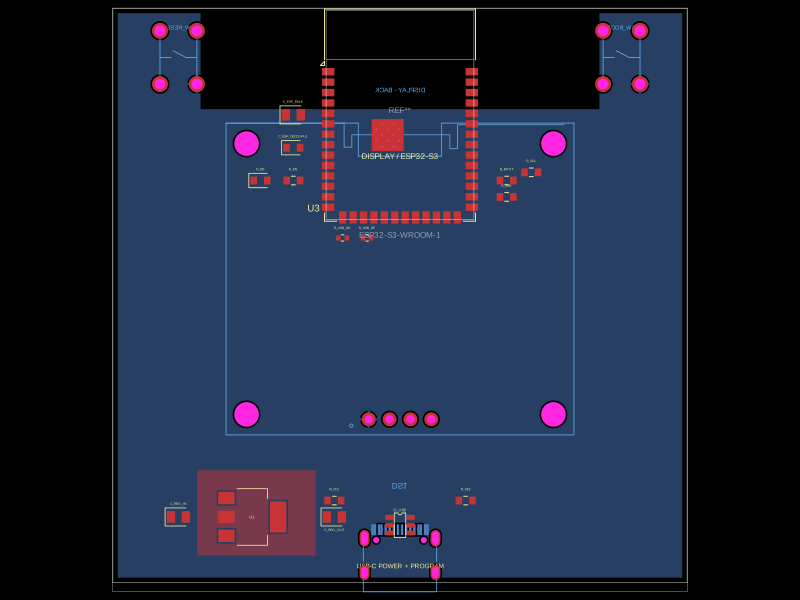
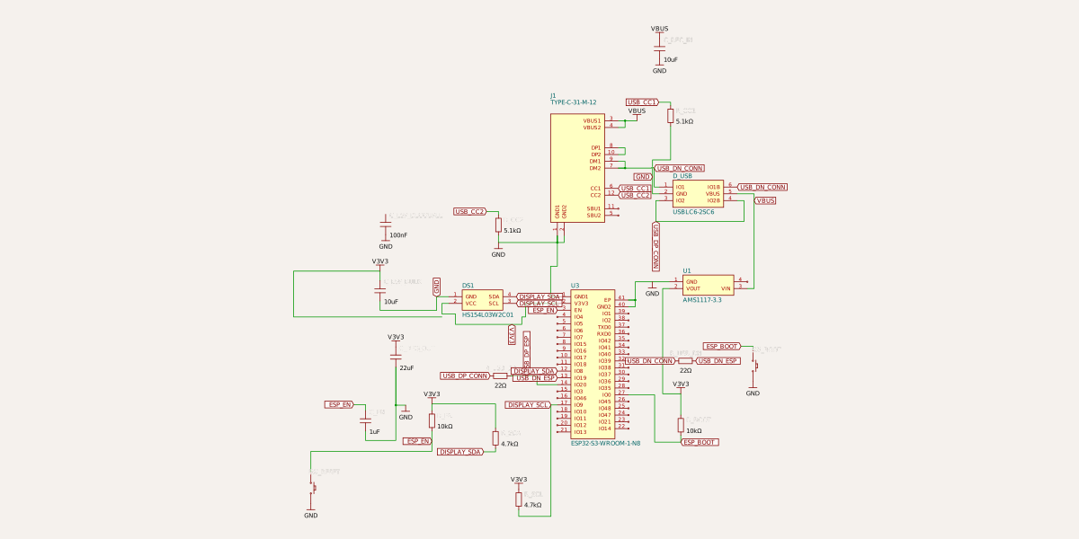
This design integrates an ESP32-S3 Wi-Fi and Bluetooth module, a USB-C port with power and data circuitry, a USB ESD protection chip, a 3.3V voltage regulator, and an OLED display module on a PCB with associated routing and thermal copper pour layers.
- Version
- 0.0.1
- License
- unset
- Stars
- 0
index.tsx
PCB
Schematic
import { SmdUsbC } from "@tsci/seveibar.smd-usb-c"
import { HS154L03W2C01 } from "./imports/c7465999"

const espPins = {
  pin1: ["GND1"], pin2: ["V3V3"], pin3: ["EN"], pin4: ["IO4"],
  pin5: ["IO5"], pin6: ["IO6"], pin7: ["IO7"], pin8: ["IO15"],
  pin9: ["IO16"], pin10: ["IO17"], pin11: ["IO18"], pin12: ["IO8"],
  pin13: ["IO19", "USB_DN"], pin14: ["IO20", "USB_DP"], pin15: ["IO3"],
  pin16: ["IO46"], pin17: ["IO9"], pin18: ["IO10"], pin19: ["IO11"],
  pin20: ["IO12"], pin21: ["IO13"], pin22: ["IO14"], pin23: ["IO21"],
  pin24: ["IO47"], pin25: ["IO48"], pin26: ["IO45"], pin27: ["IO0", "BOOT"],
  pin28: ["IO35"], pin29: ["IO36"], pin30: ["IO37"], pin31: ["IO38"],
  pin32: ["IO39"], pin33: ["IO40"], pin34: ["IO41"], pin35: ["IO42"],
  pin36: ["RXD0", "IO44"], pin37: ["TXD0", "IO43"], pin38: ["IO2"],
  pin39: ["IO1"], pin40: ["GND2"], pin41: ["EP", "GND3"],
} as const

const unusedEspPins = [
  "IO4", "IO5", "IO6", "IO7", "IO15", "IO16", "IO17", "IO18",
  "IO3", "IO46", "IO10", "IO11", "IO12", "IO13", "IO14", "IO21",
  "IO47", "IO48", "IO45", "IO35", "IO36", "IO37", "IO38", "IO39",
  "IO40", "IO41", "IO42", "RXD0", "TXD0", "IO2", "IO1",
]

export default function DisplayBoard() {
  return (
    <board width="70mm" height="70mm">
      {/* One USB-C connector for both 5 V power and native USB programming. */}
      <SmdUsbC name="J1" pcbX={0} pcbY={-31}
      noConnect={["SBU1", "SBU2"]}
      layer="bottom"
        connections={{
          A1: "net.GND", B12: "net.GND", A12: "net.GND", B1: "net.GND",
          A4: "net.VBUS", B9: "net.VBUS", A9: "net.VBUS", B4: "net.VBUS",
          A6: "net.USB_DP_CONN", B6: "net.USB_DP_CONN",
          A7: "net.USB_DN_CONN", B7: "net.USB_DN_CONN",
          CC1: "net.USB_CC1", CC2: "net.USB_CC2",
        }} />
      <resistor name="R_CC1" resistance="5.1k" footprint="0603" pcbX={-8} pcbY={-25}
        connections={{ pin1: "net.USB_CC1", pin2: "net.GND" }} />
      <resistor name="R_CC2" resistance="5.1k" footprint="0603" pcbX={8} pcbY={-25}
        connections={{ pin1: "net.USB_CC2", pin2: "net.GND" }} />

      {/* Put these 22 ohm resistors close to U3 pins 13 and 14. */}
      <resistor name="R_USB_DN" resistance="22" footprint="0402" pcbX={-7} pcbY={7}
        connections={{ pin1: "net.USB_DN_CONN", pin2: "net.USB_DN_ESP" }} />
      <resistor name="R_USB_DP" resistance="22" footprint="0402" pcbX={-4} pcbY={7}
        connections={{ pin1: "net.USB_DP_CONN", pin2: "net.USB_DP_ESP" }} />

      {/* USB ESD protection. */}
      <chip name="D_USB" manufacturerPartNumber="USBLC6-2SC6" footprint="sot23_6"
        pcbX={0} pcbY={-28}
        pinLabels={{ pin1: "IO1", pin2: "GND", pin3: "IO2", pin4: "IO2B", pin5: "VBUS", pin6: "IO1B" }}
        connections={{ IO1: "net.USB_DN_CONN", IO1B: "net.USB_DN_CONN",
          IO2: "net.USB_DP_CONN", IO2B: "net.USB_DP_CONN", GND: "net.GND", VBUS: "net.VBUS" }} />

      {/* USB 5 V to 3.3 V regulator. The large tab is also VOUT. */}
      <chip name="U1" manufacturerPartNumber="AMS1117-3.3"
        footprint="sot223" pcbX={-18} pcbY={-27}
        pinLabels={{ pin1: "GND", pin2: "VOUT", pin3: "VIN" }}
        connections={{ GND: "net.GND", VIN: "net.VBUS", VOUT: "net.V3V3" }} />
      <capacitor name="C_REG_IN" capacitance="10uF" footprint="0805"
        pcbX={-27} pcbY={-27}
        connections={{ pin1: "net.VBUS", pin2: "net.GND" }} />
      <capacitor name="C_REG_OUT" capacitance="22uF" footprint="0805"
        pcbX={-8} pcbY={-27}
        connections={{ pin1: "net.V3V3", pin2: "net.GND" }} />

      {/* ESP32-S3-WROOM-1. Antenna faces the top board edge. */}
      <chip name="U3" manufacturerPartNumber="ESP32-S3-WROOM-1-N8"
        footprint="kicad:RF_Module/ESP32-S3-WROOM-1" pcbX={0} pcbY={22}
        pinLabels={espPins} noConnect={unusedEspPins}
        connections={{ GND1: "net.GND", GND2: "net.GND", GND3: "net.GND",
          V3V3: "net.V3V3", EN: "net.ESP_EN", BOOT: "net.ESP_BOOT",
          USB_DN: "net.USB_DN_ESP", USB_DP: "net.USB_DP_ESP",
          IO8: "net.DISPLAY_SDA", IO9: "net.DISPLAY_SCL" }} />
      <capacitor name="C_ESP_BULK" capacitance="10uF" footprint="0805" pcbX={-13} pcbY={22}
        connections={{ pin1: "net.V3V3", pin2: "net.GND" }} />
      <capacitor name="C_ESP_DECOUPLE" capacitance="100nF" footprint="0603" pcbX={-13} pcbY={18}
        connections={{ pin1: "net.V3V3", pin2: "net.GND" }} />
      <resistor name="R_EN" resistance="10k" footprint="0603" pcbX={-13} pcbY={14}
        connections={{ pin1: "net.V3V3", pin2: "net.ESP_EN" }} />
      <capacitor
  name="C_EN"
  capacitance="1uF"
  footprint="0603"
  pcbX={-17}
  pcbY={14}
  connections={{
    pin1: "net.ESP_EN",
    pin2: "net.GND",
  }}
/>
      <resistor name="R_BOOT" resistance="10k" footprint="0603" pcbX={13} pcbY={14}
        connections={{ pin1: "net.V3V3", pin2: "net.ESP_BOOT" }} />
      <pushbutton name="SW_RESET" footprint="pushbutton_id1.3mm_od2mm" pcbX={-27} pcbY={29}
      layer="bottom"
        connections={{ pin1: "net.ESP_EN", pin2: "net.GND" }} />
      <pushbutton name="SW_BOOT" footprint="pushbutton_id1.3mm_od2mm" pcbX={27} pcbY={29}
      layer="bottom"
        connections={{ pin1: "net.ESP_BOOT", pin2: "net.GND" }} />

      <resistor name="R_SDA" resistance="4.7k" footprint="0603" pcbX={13} pcbY={12}
        connections={{ pin1: "net.V3V3", pin2: "net.DISPLAY_SDA" }} />
     <resistor
  name="R_SCL"
  resistance="4.7k"
  footprint="0603"
  pcbX={16}
  pcbY={15}
  connections={{
    pin1: "net.V3V3",
    pin2: "net.DISPLAY_SCL",
  }}
/>

      {/* Imported OLED module mounted directly on the back, without a pin header. */}
      <HS154L03W2C01 name="DS1" pcbX={0} pcbY={2} pcbRotation="180deg" layer="bottom"
        connections={{ GND: "net.GND", VCC: "net.V3V3",
          SCL: "net.DISPLAY_SCL", SDA: "net.DISPLAY_SDA" }} />


      {/* Explicit PCB routing. Each logical net must have physical traces. */}
      <trace from="J1.A1" to="net.GND" />
      <trace from="J1.B12" to="net.GND" />
      <trace from="J1.A12" to="net.GND" />
      <trace from="J1.B1" to="net.GND" />
      <trace from="J1.A4" to="net.VBUS"  thickness="0.8mm" />
      <trace from="J1.B9" to="net.VBUS"  thickness="0.8mm" />
      <trace from="J1.A9" to="net.VBUS"  thickness="0.8mm" />
      <trace from="J1.B4" to="net.VBUS"  thickness="0.8mm" />
      <trace from="J1.A6" to="net.USB_DP_CONN" />
      <trace from="J1.B6" to="net.USB_DP_CONN" />
      <trace from="J1.A7" to="net.USB_DN_CONN" />
      <trace from="J1.B7" to="net.USB_DN_CONN" />
      <trace from="J1.CC1" to="net.USB_CC1" />
      <trace from="R_CC1.pin1" to="net.USB_CC1" />
      <trace from="J1.CC2" to="net.USB_CC2" />
      <trace from="R_CC2.pin1" to="net.USB_CC2" />
      <trace from="R_CC1.pin2" to="net.GND" />
      <trace from="R_CC2.pin2" to="net.GND" />

      <trace from="D_USB.IO1" to="net.USB_DN_CONN" />
      <trace from="D_USB.IO1B" to="net.USB_DN_CONN" />
      <trace from="D_USB.IO2" to="net.USB_DP_CONN" />
      <trace from="D_USB.IO2B" to="net.USB_DP_CONN" />
      <trace from="D_USB.GND" to="net.GND" />
      <trace from="D_USB.VBUS" to="net.VBUS"  thickness="0.8mm" />
      <trace name="USB_DN_CONN_PAIR" from="R_USB_DN.pin1" to="net.USB_DN_CONN" thickness="0.2mm" />
      <trace name="USB_DP_CONN_PAIR" from="R_USB_DP.pin1" to="net.USB_DP_CONN" thickness="0.2mm" />
      <trace name="USB_DN_ESP_PAIR" from="R_USB_DN.pin2" to="net.USB_DN_ESP" thickness="0.2mm" />
      <trace from="U3.USB_DN" to="net.USB_DN_ESP" />
      <trace name="USB_DP_ESP_PAIR" from="R_USB_DP.pin2" to="net.USB_DP_ESP" thickness="0.2mm" />
      <trace from="U3.USB_DP" to="net.USB_DP_ESP" />

      <trace from="U1.VIN" to="net.VBUS"  thickness="0.8mm" />
      <trace from="U1.GND" to="net.GND" />
      <trace from="U1.VOUT" to="net.V3V3"  thickness="0.7mm" />
      <trace from="C_REG_IN.pin1" to="net.VBUS"  thickness="0.8mm" />
      <trace from="C_REG_IN.pin2" to="net.GND" />
      <trace from="C_REG_OUT.pin1" to="net.V3V3"  thickness="0.7mm" />
      <trace from="C_REG_OUT.pin2" to="net.GND" />

      <trace from="U3.GND1" to="net.GND" />
      <trace from="U3.GND2" to="net.GND" />
      <trace from="U3.GND3" to="net.GND" />
      <trace from="U3.V3V3" to="net.V3V3"  thickness="0.7mm" />
      <trace from="C_ESP_BULK.pin1" to="net.V3V3"  thickness="0.7mm" />
      <trace from="C_ESP_BULK.pin2" to="net.GND" />
      <trace from="C_ESP_DECOUPLE.pin1" to="net.V3V3"  thickness="0.7mm" />
      <trace from="C_ESP_DECOUPLE.pin2" to="net.GND" />
      <trace from="R_EN.pin1" to="net.V3V3"  thickness="0.7mm" />
      <trace from="R_EN.pin2" to="net.ESP_EN" />
      <trace from="U3.EN" to="net.ESP_EN" />
      <trace from="C_EN.pin1" to="net.ESP_EN" />
      <trace from="C_EN.pin2" to="net.GND" />
      <trace from="SW_RESET.pin1" to="net.ESP_EN" />
      <trace from="SW_RESET.pin2" to="net.GND" />
      <trace from="R_BOOT.pin1" to="net.V3V3"  thickness="0.7mm" />
      <trace from="R_BOOT.pin2" to="net.ESP_BOOT" />
      <trace from="U3.BOOT" to="net.ESP_BOOT" />
      <trace from="SW_BOOT.pin1" to="net.ESP_BOOT" />
      <trace from="SW_BOOT.pin2" to="net.GND" />

      <trace from="U3.IO8" to="net.DISPLAY_SDA" />
      <trace from="U3.IO9" to="net.DISPLAY_SCL" />
      <trace from="R_SDA.pin1" to="net.V3V3"  thickness="0.7mm" />
      <trace from="R_SDA.pin2" to="net.DISPLAY_SDA" />
      <trace from="R_SCL.pin1" to="net.V3V3"  thickness="0.7mm" />
      <trace from="R_SCL.pin2" to="net.DISPLAY_SCL" />
      <trace from="DS1.VCC" to="net.V3V3"  thickness="0.7mm" />
      <trace from="DS1.GND" to="net.GND" />
      <trace from="DS1.SDA" to="net.DISPLAY_SDA" />
      <trace from="DS1.SCL" to="net.DISPLAY_SCL" />

      {/* USB 2.0 differential-pair constraints. Final width/gap must be verified against the fab stack-up. */}
      <differentialpair name="USB_CONN_DIFF"
        positiveConnection="USB_DP_CONN_PAIR"
        negativeConnection="USB_DN_CONN_PAIR"
        targetDifferentialImpedance="90ohm"
        pcbTraceGap="0.2mm"
        maxLengthSkew="0.25mm"
        maxUncoupledLength="2mm" />
      <differentialpair name="USB_ESP_DIFF"
        positiveConnection="USB_DP_ESP_PAIR"
        negativeConnection="USB_DN_ESP_PAIR"
        targetDifferentialImpedance="90ohm"
        pcbTraceGap="0.2mm"
        maxLengthSkew="0.25mm"
        maxUncoupledLength="2mm" />

      {/* Local V3V3 copper heat spreader for the AMS1117 VOUT/tab. */}
      <copperpour name="AMS1117_V3V3_HEAT_SPREADER"
        layer="top"
        connectsTo="net.V3V3"
        useThermalReliefs={false}
        clearance="0.2mm"
        boardEdgeMargin="0.3mm"
        outline={[
          { x: -25, y: -32 },
          { x: -10, y: -32 },
          { x: -10, y: -21 },
          { x: -25, y: -21 },
        ]} />

      {/* Solid bottom GND plane with thermal relief. */}
      <copperpour name="GND_PLANE_BOTTOM"
        layer="bottom"
        connectsTo="net.GND"
        useThermalReliefs={true}
        unbroken={true}
        clearance="0.2mm"
        boardEdgeMargin="0.3mm"
        padMargin="0.2mm"
        traceMargin="0.2mm"
        outline={[
          { x: -34.7, y: -34.7 },
          { x: 34.7, y: -34.7 },
          { x: 34.7, y: 34.7 },
          { x: 24, y: 34.7 },
          { x: 24, y: 23 },
          { x: -24, y: 23 },
          { x: -24, y: 34.7 },
          { x: -34.7, y: 34.7 },
        ]} />
      <silkscreentext text="DISPLAY / ESP32-S3" pcbX={0} pcbY={17} fontSize="1mm" />
      <silkscreentext text="USB-C POWER + PROGRAM" pcbX={0} pcbY={-33} fontSize="0.8mm" />
      <silkscreentext text="DISPLAY - BACK" pcbX={0} pcbY={25} rotate="180deg" fontSize="0.8mm" layer="bottom" />
    </board>
  )
}