glauber/sois-controller-rev-c
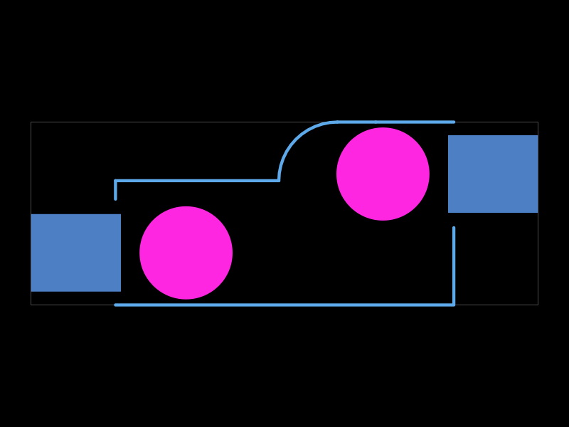
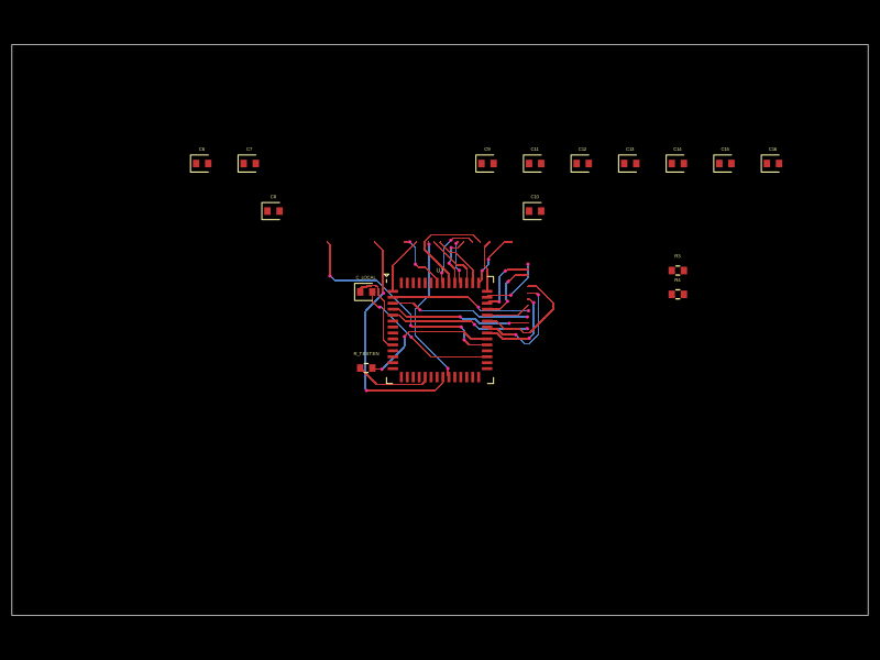
Source code for the SOIS Controller PCB, featuring an Adafruit Feather microcontroller, two EC11 rotary encoders, multiple push buttons and a slide switch. View more at glauber.org
- Version
- 0.1.3
- License
- UNLICENSED
- Stars
- 0
src/SlideSwitchCK.tsx
import type { ChipProps } from "tscircuit"
import { modelUrl } from "./models"

/**
 * C&K OS102011MA1QS1 right-angle SPDT slide switch. No KiCad library part
 * exists; this is drawn from the vendor's EasyEDA CAD for C226259, which
 * overrides the datasheet in one way that matters: the pin holes are SLOTS
 * (0.80 x 1.00), not the "3X Ø0.80" round holes the drawing calls out. The
 * terminals are 0.30 x 1.20 blades and will not enter a round 0.8mm hole.
 *
 * Drawn in board orientation — hole line along y, actuator projecting -x
 * through the left board edge — so it is placed unrotated.
 *
 * Pin 2 (common) = EN, pin 3 = GND, pin 1 = NC. Sliding toward pin 3 pulls the
 * Feather's EN low and the box is off, on battery and USB alike.
 */

const pinLabels = { pin1: "NC", pin2: "COM", pin3: "SEL" } as const

/** All five holes are collinear; origin is pad 2, the common. */
const PIN_DY = 2.0
const PEG_DY = 4.201

export const SlideSwitchCK = (props: ChipProps<typeof pinLabels>) => (
  <chip
    {...props}
    pinLabels={pinLabels}
    manufacturerPartNumber="OS102011MA1QS1"
    supplierPartNumbers={{ jlcpcb: ["C221530"] }}
    cadModel={{
      stepUrl: modelUrl("ck_os102011_switch.step"),
      rotationOffset: { x: 0, y: 0, z: -90 },
      positionOffset: { x: 0, y: 0, z: 1.97 },
    }}
    footprint={
      // Pressed in from above, actuated sideways, so the enclosure opening
      // follows the actuator rather than the insertion.
      <footprint insertionDirection="from_above" cutoutApertureDirection="from_left">
        {([
          ["1", PIN_DY],
          ["2", 0],
          ["3", -PIN_DY],
        ] as Array<[string, number]>).map(([hint, y]) => (
          <platedhole
            key={hint}
            portHints={[hint]}
            shape="pill"
            pcbX="0mm"
            pcbY={`${y}mm`}
            outerWidth="1.3mm"
            outerHeight="1.6mm"
            holeWidth="0.8mm"
            holeHeight="1mm"
          />
        ))}
        {/* Locating pegs: NPTH, slots across the hole line. */}
        {[PEG_DY, -PEG_DY].map((y) => (
          <hole key={y} shape="pill" width="1.8mm" height="1.1mm" pcbX="0mm" pcbY={`${y}mm`} />
        ))}
        {/* 8.63 x 4.59 body, centred on the hole line. */}
        <silkscreenpath
          strokeWidth="0.12mm"
          route={[
            { x: -2.3, y: 4.31 },
            { x: 2.3, y: 4.31 },
            { x: 2.3, y: -4.31 },
            { x: -2.3, y: -4.31 },
            { x: -2.3, y: 4.31 },
          ]}
        />
      </footprint>
    }
  />
)