glauber/sois-controller-rev-c
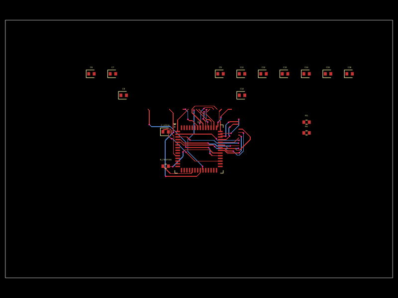
Source code for the SOIS Controller PCB, featuring an Adafruit Feather microcontroller, two EC11 rotary encoders, multiple push buttons and a slide switch. View more at glauber.org
- Version
- 0.1.3
- License
- UNLICENSED
- Stars
- 0
src/EC11Encoder.tsx
import type { ChipProps } from "tscircuit"
import { modelUrl } from "./models"

/**
 * Alps EC11E15244G1 vertical click-encoder, from KiCad's
 * `Rotary_Encoder:RotaryEncoder_Alps_EC11E-Switch_Vertical_H20mm`. Local y is
 * negated from the .kicad_mod.
 *
 * Footprint origin is pad A; the shaft axis is at local (7.5, -2.5). A/B/C are
 * the quadrature contacts (C common), S1/S2 the push switch, MP the two frame
 * tabs — one port, two holes, on GND so the metal body is grounded.
 *
 * The MP tabs are rect pads over slots in the library, drawn here as plain
 * pills: same hole, same envelope, corners rounded off.
 */

const pinLabels = {
  pin1: "A",
  pin2: "B",
  pin3: "C",
  pin4: "S1",
  pin5: "S2",
  pin6: "MP",
} as const

export const EC11Encoder = (props: ChipProps<typeof pinLabels>) => (
  <chip
    {...props}
    pinLabels={pinLabels}
    manufacturerPartNumber="EC11E15244G1"
    // GENERATED by ../controller-rev-c/3dmodels/make_models.py from the Alps
    // catalogue drawing, in the FOOTPRINT's own frame (origin = shaft axis at
    // z=0), so no rotation is needed. Shaft tip at 24.5mm: 4.5 body + 7.0 Ø7
    // bushing + 13.0 Ø6 shaft, flat over the top 10mm.
    cadModel={{
      stepUrl: modelUrl("ec11_encoder.step"),
      // Shaft axis is 0.25mm off the pad-bbox centre the model anchors on.
      positionOffset: { x: 0.25, y: 0, z: 0 },
    }}
    footprint={
      <footprint>
        <platedhole
          portHints={["1", "A"]}
          shape="circular_hole_with_rect_pad"
          pcbX="0mm"
          pcbY="0mm"
          holeDiameter="1mm"
          rectPadWidth="2mm"
          rectPadHeight="2mm"
        />
        <platedhole
          portHints={["2", "B"]}
          shape="circle"
          pcbX="0mm"
          pcbY="-5mm"
          holeDiameter="1mm"
          outerDiameter="2mm"
        />
        <platedhole
          portHints={["3", "C"]}
          shape="circle"
          pcbX="0mm"
          pcbY="-2.5mm"
          holeDiameter="1mm"
          outerDiameter="2mm"
        />
        <platedhole
          portHints={["4", "S1"]}
          shape="circle"
          pcbX="14.5mm"
          pcbY="-5mm"
          holeDiameter="1mm"
          outerDiameter="2mm"
        />
        <platedhole
          portHints={["5", "S2"]}
          shape="circle"
          pcbX="14.5mm"
          pcbY="0mm"
          holeDiameter="1mm"
          outerDiameter="2mm"
        />
        {/* Frame tabs: slotted holes, both on the same port. */}
        <platedhole
          portHints={["6", "MP"]}
          shape="pill"
          pcbX="7.5mm"
          pcbY="3.1mm"
          holeWidth="2.8mm"
          holeHeight="1.5mm"
          outerWidth="3.2mm"
          outerHeight="2mm"
        />
        <platedhole
          portHints={["6", "MP"]}
          shape="pill"
          pcbX="7.5mm"
          pcbY="-8.1mm"
          holeWidth="2.8mm"
          holeHeight="1.5mm"
          outerWidth="3.2mm"
          outerHeight="2mm"
        />
        {/* 12.4 x 11.4 body */}
        <silkscreenpath
          strokeWidth="0.12mm"
          route={[
            { x: 1.3, y: 3.2 },
            { x: 13.7, y: 3.2 },
            { x: 13.7, y: -8.2 },
            { x: 1.3, y: -8.2 },
            { x: 1.3, y: 3.2 },
          ]}
        />
      </footprint>
    }
  />
)