glauber/sois-controller-rev-c
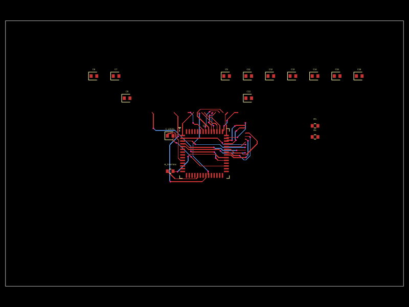
Source code for the SOIS Controller PCB, featuring an Adafruit Feather microcontroller, two EC11 rotary encoders, multiple push buttons and a slide switch. View more at glauber.org
- Version
- 0.1.3
- License
- UNLICENSED
- Stars
- 0
src/AdafruitFeather.tsx
import type { ChipProps } from "tscircuit"
import { modelUrl } from "./models"

/**
 * Adafruit Feather (ESP32-S3), from KiCad's
 * `Module:Adafruit_Feather_WithMountingHoles`. Local y is negated from the
 * .kicad_mod (KiCad y-down -> tscircuit y-up).
 *
 * Pads are drawn centred on their holes. The library nudges each pad's copper
 * 0.3mm inboard of its drill, but no tscircuit plated-hole shape can carry
 * that offset correctly on a rotated component, so the holes are placed
 * exactly and the copper is left symmetric. That also makes pad 1 oval rather
 * than rectangular, so the pin-1 marker is drawn on the silkscreen.
 *
 * Only pin names verified against Adafruit's pinout are given; pads 3 and
 * 9-16 stay numeric, and nothing on this board connects to them.
 */

const PAD_W = 2.6
const PAD_H = 1.6
const HOLE_D = 1.0
/** 16-pin row at local x=0, pin 1 at the USB end; 12-pin row at x=20.32. */
const ROW_X = 20.32
const PITCH = 2.54

const pinLabels = {
  pin1: "RST",
  pin2: "V3_3",
  pin4: "GND",
  pin5: "A0",
  pin6: "A1",
  pin7: "A2",
  pin8: "A3",
  pin17: "SDA",
  pin18: "SCL",
  pin19: "D5",
  pin20: "D6",
  pin21: "D9",
  pin22: "D10",
  pin23: "D11",
  pin24: "D12",
  pin25: "D13",
  pin26: "VBUS",
  pin27: "EN",
  pin28: "VBAT",
} as const

/** [pad number, local x, local y (already y-up), reserved] */
const pads: Array<[number, number, number, number]> = [
  // 16-pin row, running away from the USB end.
  ...Array.from({ length: 16 }, (_, i): [number, number, number, number] => [
    i + 1,
    0,
    -(i * PITCH),
    0,
  ]),
  // 12-pin row, running back toward it.
  ...Array.from({ length: 12 }, (_, i): [number, number, number, number] => [
    i + 17,
    ROW_X,
    -(38.1 - i * PITCH),
    0,
  ]),
]

/** The module's own NPTH mounting holes. */
const mountingHoles: Array<[number, number, number]> = [
  [1.27, 3.81, 2.5],
  [19.05, 3.81, 2.5],
  [1.27, -41.91, 2.54],
  [19.05, -41.91, 2.54],
]

export const AdafruitFeather = (props: ChipProps<typeof pinLabels>) => (
  <chip
    {...props}
    pinLabels={pinLabels}
    manufacturerPartNumber="ADAFRUIT-5323"
    cadModel={{
      stepUrl: modelUrl("feather-5323.step"),
      rotationOffset: { x: 0, y: 0, z: -90 },
    // Model origin is the module corner; shift back by half of 50.8 x 22.86.
      positionOffset: { x: -25.4, y: -11.43, z: 0 },
    }}
    footprint={
      <footprint>
        {pads.map(([n, x, y]) => (
          <platedhole
            key={n}
            portHints={[`${n}`]}
            shape="pill"
            pcbX={`${x}mm`}
            pcbY={`${y}mm`}
            outerWidth={`${PAD_W}mm`}
            outerHeight={`${PAD_H}mm`}
            holeWidth={`${HOLE_D}mm`}
            holeHeight={`${HOLE_D}mm`}
          />
        ))}
        {mountingHoles.map(([x, y, d], i) => (
          <hole key={`mh${i}`} shape="circle" diameter={`${d}mm`} pcbX={`${x}mm`} pcbY={`${y}mm`} />
        ))}
        {/* Pin-1 marker */}
        <silkscreenpath
          strokeWidth="0.15mm"
          route={[
            { x: -1.0, y: 1.0 },
            { x: -1.0, y: -1.0 },
            { x: -2.0, y: 0 },
            { x: -1.0, y: 1.0 },
          ]}
        />
        {/* Module outline: 0.9in x 2.0in, USB at the -44.45 end. */}
        <silkscreenpath
          strokeWidth="0.12mm"
          route={[
            { x: -1.27, y: 6.35 },
            { x: 21.59, y: 6.35 },
            { x: 21.59, y: -44.45 },
            { x: -1.27, y: -44.45 },
            { x: -1.27, y: 6.35 },
          ]}
        />
      </footprint>
    }
  />
)