glauber/sois-controller-rev-c
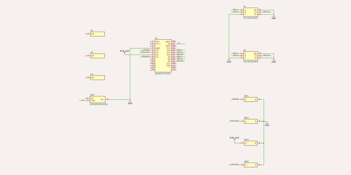
Source code for the SOIS Controller PCB, featuring an Adafruit Feather microcontroller, two EC11 rotary encoders, multiple push buttons and a slide switch. View more at glauber.org
- Version
- 0.1.3
- License
- UNLICENSED
- Stars
- 0
index.circuit.tsx
PCB
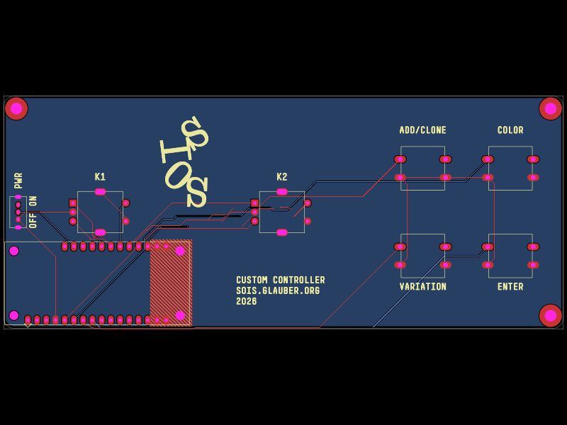
Schematic
import {
  ANT_KEEPOUT,
  CORNER_HOLES,
  CORNER_RADIUS,
  EC11_SHAFT_OFF,
  FEATHER,
  FEATHER_ROT,
  H,
  KNOBS,
  SW5,
  SW_CELL,
  SW_OFF,
  W,
  bx,
  by,
} from "./src/geometry"
import { AdafruitFeather } from "./src/AdafruitFeather"
import { EC11Encoder } from "./src/EC11Encoder"
import { PushButton12mm } from "./src/PushButton12mm"
import { SlideSwitchCK } from "./src/SlideSwitchCK"
import { MountingHoleM3 } from "./src/MountingHoleM3"
import { silkArt } from "./src/silkArt"

/**
 * sois controller carrier PCB, rev C — a tscircuit port of
 * `../controller-rev-c/`, the KiCad board that was fabricated.
 *
 * Electrically it is one idea: every input shorts its GPIO to GND through a
 * contact and is read INPUT_PULLUP, so there is not a single passive on the
 * board. Encoder C and S1 sit on GND; the slide switch pulls the Feather's EN
 * low to switch the box off, on battery and USB alike.
 */

const [k1x, k1y] = KNOBS[0]
const [k2x, k2y] = KNOBS[1]
const [ax1, ay1, ax2, ay2] = ANT_KEEPOUT
/** Keyed as-is in silk.json. */
const COLOPHON = "CUSTOM CONTROLLER\nSOIS.GLAUBER.ORG\n2026"

/** Both are placed by footprint origin, so the cap-centre geometry above is
 *  offset by each part's origin-to-centre vector. */
const encoderAt = ([x, y]: [number, number]) => ({
  pcbX: bx(x - EC11_SHAFT_OFF[0]),
  pcbY: by(y - EC11_SHAFT_OFF[1]),
})
const buttonAt = ([x, y]: [number, number]) => ({
  pcbX: bx(x - SW_OFF[0]),
  pcbY: by(y - SW_OFF[1]),
})

export default () => (
  // The only placement errors on this board are false: the Ø6.2 mounting-hole
  // rings are tested as bounding boxes against the rounded outline. Left on,
  // they skip autorouting entirely.
  <board
    width={`${W}mm`}
    height={`${H}mm`}
    borderRadius={CORNER_RADIUS}
    // Black mask, white silk — what rev C was actually fabricated as, and what
    // the ordering notes in ../controller-rev-c/README.md specify.
    solderMaskColor="black"
    silkscreenColor="white"
    placementDrcChecksDisabled
  >
    {/* GND is poured, not routed — `routingPhaseIndex={null}` keeps the
        autorouter off it. */}
    <net name="GND" isGroundNet routingPhaseIndex={null} />

    <AdafruitFeather
      name="U1"
      pcbX={bx(FEATHER[0])}
      pcbY={by(FEATHER[1])}
      pcbRotation={FEATHER_ROT}
      schX={-4}
      schY={0}
      connections={{
        GND: "net.GND",
        A0: "net.BTN_ADD",
        A1: "net.BTN_COLOR",
        A2: "net.BTN_VAR",
        A3: "net.BTN_ENTER",
        D5: "net.ENC2_SW",
        D6: "net.ENC2_B",
        D9: "net.ENC2_A",
        D10: "net.ENC1_SW",
        D11: "net.ENC1_B",
        D12: "net.ENC1_A",
        EN: "net.EN",
      }}
    />

    <EC11Encoder
      name="K1"
      {...encoderAt([k1x, k1y])}
      schX={4}
      schY={4}
      connections={{
        A: "net.ENC1_A",
        B: "net.ENC1_B",
        C: "net.GND",
        S1: "net.GND",
        S2: "net.ENC1_SW",
        MP: "net.GND",
      }}
    />
    <EC11Encoder
      name="K2"
      {...encoderAt([k2x, k2y])}
      schX={4}
      schY={0}
      connections={{
        A: "net.ENC2_A",
        B: "net.ENC2_B",
        C: "net.GND",
        S1: "net.GND",
        S2: "net.ENC2_SW",
        MP: "net.GND",
      }}
    />

    <PushButton12mm name="SW1" {...buttonAt(SW_CELL[0])} schX={4} schY={-4}
      connections={{ A: "net.BTN_ADD", B: "net.GND" }} />
    <PushButton12mm name="SW2" {...buttonAt(SW_CELL[1])} schX={4} schY={-6}
      connections={{ A: "net.BTN_COLOR", B: "net.GND" }} />
    <PushButton12mm name="SW3" {...buttonAt(SW_CELL[2])} schX={4} schY={-8}
      connections={{ A: "net.BTN_VAR", B: "net.GND" }} />
    <PushButton12mm name="SW4" {...buttonAt(SW_CELL[3])} schX={4} schY={-10}
      connections={{ A: "net.BTN_ENTER", B: "net.GND" }} />

    <SlideSwitchCK
      name="SW5"
      pcbX={bx(SW5[0])}
      pcbY={by(SW5[1])}
      schX={-10}
      schY={-4}
      connections={{ COM: "net.EN", SEL: "net.GND" }}
    />

    {CORNER_HOLES.map(([x, y], i) => (
      <MountingHoleM3 key={i} name={`H${i + 1}`} pcbX={bx(x)} pcbY={by(y)} schX={-10} schY={2 - i * 2} />
    ))}

    {/* No copper under the Feather's PCB antenna, either layer. U1 is excluded
        because four of its own unconnected pads sit inside — tscircuit's
        keepout has no per-class control, so it cannot allow pads but not
        traces the way KiCad's zone does. */}
    <keepout
      shape="rect"
      width={ax2 - ax1}
      height={ay2 - ay1}
      pcbX={bx((ax1 + ax2) / 2)}
      pcbY={by((ay1 + ay2) / 2)}
      layers={["top", "bottom"]}
      excludeRefs={[".U1"]}
    />

    {/* Panel labels, positioned as on the fabricated board. */}
    {silkArt("K1", k1x, 22.2)}
    {silkArt("K2", k2x, 22.2)}
    {silkArt("ADD/CLONE", SW_CELL[0][0], SW_CELL[0][1] - 10.6)}
    {silkArt("COLOR", SW_CELL[1][0], SW_CELL[1][1] - 10.6)}
    {silkArt("VARIATION", SW_CELL[2][0], SW_CELL[2][1] + 8.4)}
    {silkArt("ENTER", SW_CELL[3][0], SW_CELL[3][1] + 8.4)}
    {silkArt("PWR", SW5[0], SW5[1] - 8.66, 90)}
    {silkArt("ON", SW5[0] + 4.0, SW5[1] - 3.04, 90)}
    {silkArt("OFF", SW5[0] + 4.0, SW5[1] + 2.34, 90)}
    {silkArt(COLOPHON, 64.17, 49.68, 0, "tl")}
    {silkArt("@logo", 49.67, 18.1, 90)}

    {/* GND pour on the back, full board less a 0.6mm edge margin. */}
    <copperpour layer="bottom" connectsTo="net.GND" boardEdgeMargin="0.6mm" />
  </board>
)