davixcky/bjt-2
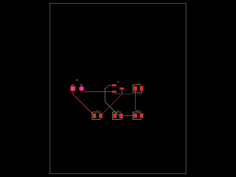
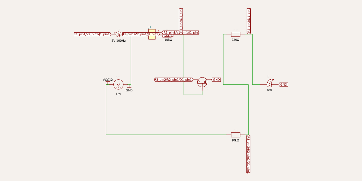
This schematic implements a transistor-driven LED indicator circuit powered by a 12V supply, with a control input via a 5V square wave signal.
- Version
- 0.0.1
- License
- unset
- Stars
- 0
index.tsx
PCB
Schematic
export default () => (
  <board width="40mm" height="50mm">
    {/* 12V Power Supply */}
    <voltagesource
      name="V1"
      voltage="12V"
      schX={-5}
      schY={0}
    />

    {/* Base resistor - limits current into transistor base */}
    <resistor
      name="R1"
      resistance="10k"
      footprint="0805"
      schX={-2}
      schY={3}
      pcbX={-6}
      pcbY={-8}
    />

    {/* Collector pull-up resistor */}
    <resistor
      name="R3"
      resistance="10k"
      footprint="0805"
      schX={2}
      schY={-3}
      pcbX={0}
      pcbY={-8}
    />

    {/* LED current limiting resistor */}
    <resistor
      name="R2"
      resistance="220"
      footprint="0805"
      schX={2}
      schY={3}
      pcbX={6}
      pcbY={-8}
    />

    {/* NPN Transistor 2N2222 - the switch */}
    <transistor
      name="Q1"
      type="npn"
      footprint="sot23"
      schX={0}
      schY={0}
      pcbX={0}
      pcbY={0}
    />

    {/* Red LED - output indicator */}
    <led
      name="D1"
      color="red"
      footprint="0805"
      schX={4}
      schY={0}
      pcbX={6}
      pcbY={0}
    />

    {/* Square wave input for simulation: 0V to 5V at 100Hz */}
    <voltagesource
      name="V2"
      voltage="5V"
      waveShape="square"
      frequency="100"
      dutyCycle="0.5"
      schX={-5}
      schY={3}
    />

    {/* Physical input connector (2-pin header) */}
    <pinheader
      name="J1"
      pinCount={2}
      footprint="pinrow2"
      schX={-3}
      schY={3}
      pcbX={-12}
      pcbY={0}
    />

    {/* V2 drives J1 in simulation */}
    <trace from=".V2 > .pin1" to=".J1 > .pin1" />
    <trace from=".V2 > .pin2" to="net.GND" />

    {/* Input signal -> R1 -> Base */}
    <trace from=".J1 > .pin1" to=".R1 > .pin1" />
    <trace from=".J1 > .pin2" to="net.GND" />
    <trace from=".R1 > .pin2" to=".Q1 > .base" />

    {/* V1 positive (pin1) -> R3 (pull-up) */}
    <trace from=".V1 > .pin1" to="net.VCC12" />
    <trace from="net.VCC12" to=".R3 > .pin1" />

    {/* R3 -> R2 -> LED anode (collector node) */}
    <trace from=".R3 > .pin2" to=".Q1 > .collector" />
    <trace from=".R3 > .pin2" to=".R2 > .pin1" />
    <trace from=".R2 > .pin2" to=".D1 > .anode" />

    {/* LED cathode -> GND */}
    <trace from=".D1 > .cathode" to="net.GND" />

    {/* Transistor emitter -> GND */}
    <trace from=".Q1 > .emitter" to="net.GND" />

    {/* V1 negative (pin2) -> GND */}
    <trace from=".V1 > .pin2" to="net.GND" />

    {/* SPICE transient analysis: 20ms simulation, 10µs steps */}
    <analogsimulation
      simulationType="spice_transient_analysis"
      duration="20ms"
      timePerStep="10us"
    />
  </board>
)