astrimid/ec_driven_dc_isolation
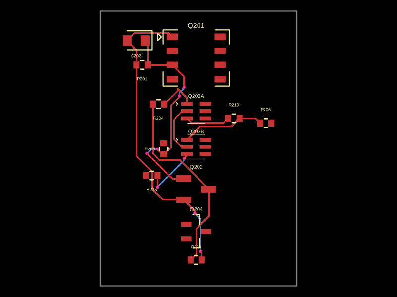
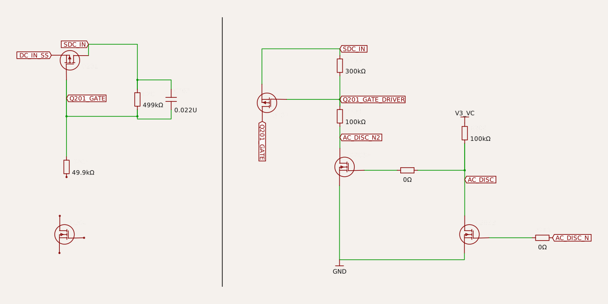
This code models a power control circuit featuring NPN and P-channel MOSFETs, resistors, and capacitors, including a dual N-channel MOSFET package, to manage power paths and switching functions on a hardware PCB.
- Version
- 0.0.1
- License
- unset
- Stars
- 0
index.tsx
PCB
Schematic
import { Subcircuit } from "tscircuit"

const Dmn65D8LdwPackage = ({ name, mfg, mpn, footprint }) => {
  return (
    <subcircuit>
      {/* 1. The physical anchor: Handles footprint, BOM tracking, and manufacturer data */}
      <chip
        name={name}
        manufacturerPartNumber={mpn}
        footprint={footprint}
        pinLabels={{
          1: "S1", // Source 1
          2: "G1", // Gate 1
          3: "D2", // Drain 2
          4: "S2", // Source 2
          5: "G2", // Gate 2
          6: "D1", // Drain 1
        }}
      />

      {/* 2. Visual Channel A: Rendered as a distinct MOSFET symbol */}
      <mosfet
        name={`${name}A`}
        channelType="n"
        mosfetMode="enhancement"
        symbolDrainSide="top"
        symbolSourceSide="bottom"
        symbolGateSide="right"
        schSectionName="ac_disc_path"
        schRotation={0}
        schX={2.3}
        schY={13}
      />

      {/* 3. Visual Channel B: Rendered as a distinct MOSFET symbol */}
      <mosfet
        name={`${name}B`}
        channelType="n"
        mosfetMode="enhancement"
        symbolGateSide="right"
        schSectionName="ac_disc_path"
        schX={6}
        schY={11}
      />

      {/* 4. Internal Mapping: Links physical chip pads to the visual schematic nodes */}
      {/* Channel A internal layout links */}
      <net from={`${name}.pin2`} to={`${name}A.gate`} />
      <net from={`${name}.pin1`} to={`${name}A.source`} />
      <net from={`${name}.pin6`} to={`${name}A.drain`} />

      {/* Channel B internal layout links */}
      <net from={`${name}.pin5`} to={`${name}B.gate`} />
      <net from={`${name}.pin4`} to={`${name}B.source`} />
      <net from={`${name}.pin3`} to={`${name}B.drain`} />
    </subcircuit>
  )
}

export const PowerPathControl = () => (
  <board routingDisabled={false} schMaxTraceDistance={1000}>
    {/* ============================================================ */}
    {/* 1. Global Setup & Definitions                                */}
    {/* ============================================================ */}
    <schematicsection name="dc_in_ss_path" />
    <schematicsection name="ac_disc_path" />

    <net name="GND" />

    {/* ============================================================ */}
    {/* 2. DC Input Soft Start Path (dc_in_ss_path)                  */}
    {/* ============================================================ */}

    {/* Components */}
    <mosfet
      name="Q201"
      manufacturerPartNumber="AON7409"
      channelType="p"
      mosfetMode="enhancement"
      footprint="dfn8-5"
      symbolGateSide="bottom"
      symbolSourceSide="left"
      schSectionName="dc_in_ss_path"
      schX={-6}
      schY={16}
    />

    <resistor
      name="R201"
      resistance="499k"
      footprint="0402"
      schSectionName="dc_in_ss_path"
      schRotation={90}
      schX={-4}
      schY={15}
    />

    <capacitor
      name="C202"
      capacitance="0.022U"
      footprint="0603"
      schSectionName="dc_in_ss_path"
      schRotation={90}
      schX={-3}
      schY={15}
    />

    <resistor
      name="R205"
      resistance="49.9k"
      footprint="0402"
      schSectionName="dc_in_ss_path"
      schRotation={-90}
      schX={-6.1}
      schY={13}
    />

    {/* Connectivity */}
    <trace from=".Q201 .source" to="net.DC_IN_SS" />
    <trace from=".Q201 .drain" to="net.SDC_IN" />
    <trace from=".R201 .pin2" to="net.SDC_IN" />
    <trace from=".R201 .pin1" to=".Q201 .gate" />
    <trace from=".C202 .pin2" to="net.SDC_IN" />
    <trace from=".C202 .pin1" to=".Q201 .gate" />
    <trace from=".R205 .pin1" to=".Q201 .gate" />


    {/* ============================================================ */}
    {/* 3. AC Disconnect Path (ac_disc_path)                         */}
    {/* ============================================================ */}

    {/* Components */}
    <mosfet
      name="Q202"
      manufacturerPartNumber="AO3409"
      channelType="p"
      mosfetMode="enhancement"
      footprint="sot23"
      symbolGateSide="right"
      symbolSourceSide="top"
      schSectionName="ac_disc_path"
      schRotation={0}
      schX={0}
      schY={14.9}
    />

    <resistor
      name="R200"
      resistance="300k"
      footprint="0402"
      schSectionName="ac_disc_path"
      schRotation={90}
      schX={2}
      schY={16}
    />

    <resistor
      name="R204"
      resistance="100k"
      footprint="0402"
      schSectionName="ac_disc_path"
      schRotation={90}
      schX={2}
      schY={14.5}
    />

    {/* Q203A & Q203B: Two channels of a single dual DMN65D8LDW package */}
    <mosfet
      name="Q203A"
      manufacturerPartNumber="DMN65D8LDW"
      channelType="n"
      mosfetMode="enhancement"
      footprint="sot363"
      symbolDrainSide="top"
      symbolSourceSide="bottom"
      symbolGateSide="right"
      schSectionName="ac_disc_path"
      schRotation={0}
      schX={2.3}
      schY={13}
    />

    <resistor
      name="R210"
      resistance="0"
      footprint="0402"
      schSectionName="ac_disc_path"
      schRotation={0}
      schX={4}
      schY={12.9}
    />

    <resistor
      name="R206"
      resistance="100k"
      footprint="0402"
      schSectionName="ac_disc_path"
      schRotation={90}
      schX={5.7}
      schY={14}
    />

    <mosfet
      name="Q203B"
      manufacturerPartNumber="DMN65D8LDW"
      channelType="n"
      mosfetMode="enhancement"
      footprint="sot363"
      symbolGateSide="right"
      schSectionName="ac_disc_path"
      schX={6}
      schY={11}
    />

    <resistor
      name="R218"
      resistance="0"
      footprint="0402"
      schSectionName="ac_disc_path"
      schX={8}
      schY={10.9}
    />

    {/* Q204: Single N-Channel MOSFET (Declared for future connections) */}
    <mosfet
      name="Q204"
      manufacturerPartNumber="DMN65D8LW"
      channelType="n"
      mosfetMode="enhancement"
      footprint="sot323"
      symbolGateSide="right"
      schSectionName="dc_in_ss_path"
      schX={-6}
      schY={11}
    />

    {/* Connectivity */}
    <trace from=".Q202 .source" to="net.SDC_IN" />
    <trace from=".Q202 .gate" to="net.Q201_GATE_DRIVER" />
    <trace name="Q201_GATE" from=".Q202 .drain" to=".R205 .pin1" />

    <trace from=".R200 .pin2" to="net.SDC_IN" />
    <trace from=".R200 .pin1" to="net.Q201_GATE_DRIVER" />

    <trace from=".R204 .pin2" to="net.Q201_GATE_DRIVER" />
    <trace name="AC_DISC_N2" from=".Q203A .drain" to=".R204 .pin1" />
    <trace from=".Q203A .gate" to=".R210 .pin1" />
    <trace from=".Q203A .source" to="net.GND" />

    <trace name="AC_DISC" from=".R206 .pin1" to=".R210 .pin2" />
    <trace from=".R206 .pin2" to="net.V3_VC" />

    <trace name="AC_DISC" from=".Q203B .drain" to=".R206 .pin1" />
    <trace from=".Q203B .gate" to=".R218 .pin1" />
    <trace from=".Q203B .source" to="net.GND" />
    <trace from=".R218 .pin2" to="net.AC_DISC_N" />
  </board>
)