astrimid/dual_standby_power_example
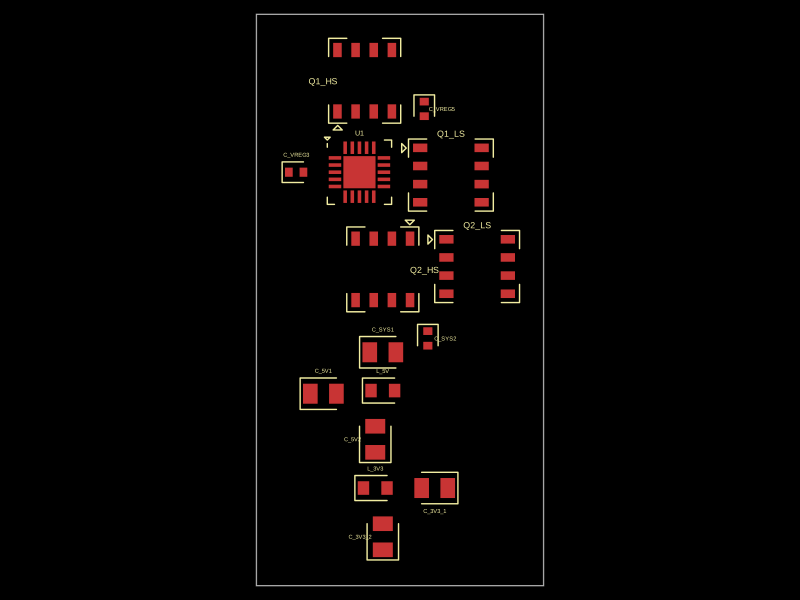
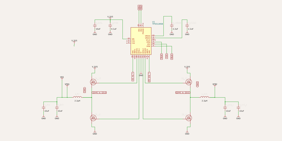
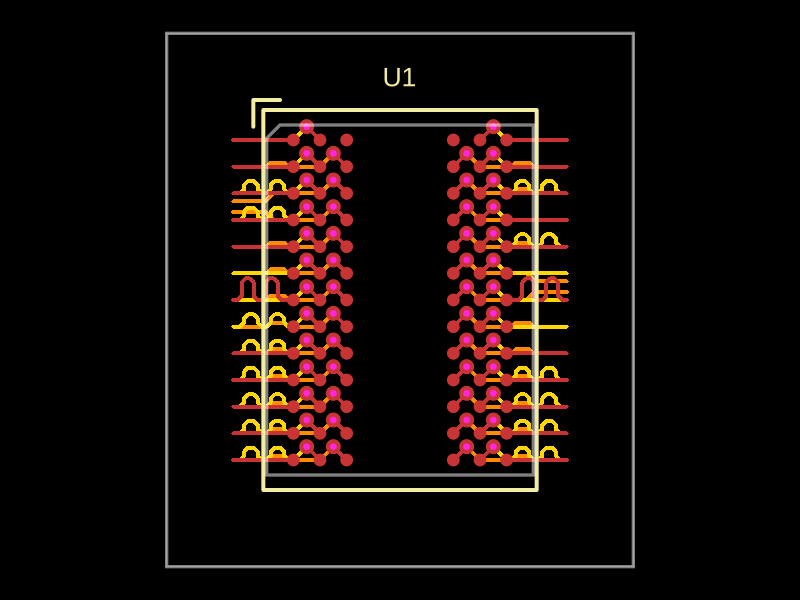
This code defines an electronic power regulation circuit comprising a TPS51285B controller, input and output filtering components, and two parallel synchronous buck converter channels generating 5V and 3.3V outputs with associated MOSFETs, inductors, and capacitors.
- Version
- 0.0.1
- License
- unset
- Stars
- 0
index.tsx
PCB
Schematic
import { TPS51285B } from "@tsci/astrimid.TPS51285B"

export const StandbyDualController = () => {
  return (
    <board schMaxTraceDistance={10} routingDisabled>
      <subcircuit schMaxTraceDistance={10}>
        {/* ================= CONTROLLER (U1) ================= */}
        <TPS51285B name="U1" schematicStyle="system" schX={0} schY={0} />
        <netlabel
          net="GND"
          connectsTo="U1.TP"
          schX={0}
          schY={-3}
          anchorSide="top"
        />

        {/* ================= INPUT & V_SYS BUS ================= */}
        <port name="V_SYS_IN" type="power_input" schX={-6.5} schY={-0.5} />
        <netlabel
          net="V_SYS"
          connectsTo=".V_SYS_IN"
          schX={-6.5}
          schY={-0.25}
          anchorSide="bottom"
        />

        <capacitor
          name="C_SYS1"
          capacitance="10uF"
          maxVoltageRating="25V"
          footprint="0805"
          schX={-4.5}
          schY={1.5}
          schRotation={90}
        />
        <capacitor
          name="C_SYS2"
          capacitance="0.1uF"
          maxVoltageRating="25V"
          footprint="0402"
          schX={-3.0}
          schY={1.5}
          schRotation={90}
        />

        <trace from=".V_SYS_IN" to="C_SYS2.pin2" />
        <trace from=".V_SYS_IN" to="C_SYS1.pin2" />
        <trace from="C_SYS1.pin2" to="C_SYS2.pin2" />
        <trace from="C_SYS2.pin2" to="U1.VIN" />

        <netlabel
          net="GND"
          connectsTo="C_SYS1.pin1"
          schX={-4.5}
          schY={1.0}
          anchorSide="top"
        />
        <netlabel
          net="GND"
          connectsTo="C_SYS2.pin1"
          schX={-3.0}
          schY={1.0}
          anchorSide="top"
        />

        <netlabel
          net="EN1"
          connectsTo="U1.EN1"
          schX={-0.2}
          schY={3}
          anchorSide="bottom"
        />
        <netlabel
          net="EN2"
          connectsTo="U1.EN2"
          schX={0}
          schY={3}
          anchorSide="bottom"
        />

        {/* ================= VREG & FEEDBACK ================= */}
        <capacitor
          name="C_VREG5"
          capacitance="2.2uF"
          maxVoltageRating="10V"
          footprint="0402"
          schX={3.0}
          schY={1.5}
          schRotation={90}
        />
        <capacitor
          name="C_VREG3"
          capacitance="2.2uF"
          maxVoltageRating="10V"
          footprint="0402"
          schX={4.5}
          schY={1.5}
          schRotation={90}
        />
        <trace from="U1.VREG5" to="C_VREG5.pin2" />
        <trace from="U1.VREG3" to="C_VREG3.pin2" />
        <netlabel
          net="GND"
          connectsTo="C_VREG5.pin1"
          schX={3.0}
          schY={1.0}
          anchorSide="top"
        />
        <netlabel
          net="GND"
          connectsTo="C_VREG3.pin1"
          schX={4.5}
          schY={1.0}
          anchorSide="top"
        />

        <netlabel
          net="VFB1"
          connectsTo="U1.VFB1"
          schX={2.0}
          schY={-1.2}
          anchorSide="top"
        />
        <netlabel
          net="VO1"
          connectsTo="U1.VO1"
          schX={2.5}
          schY={-1.2}
          anchorSide="top"
        />
        <netlabel
          net="VFB2"
          connectsTo="U1.VFB2"
          schX={3.0}
          schY={-1.2}
          anchorSide="top"
        />

        {/* ================= CHANNEL 1 (5V) - LEFT POWER STAGE ================= */}
        <mosfet
          name="Q1_HS"
          manufacturerPartNumber="CSD17578Q3A"
          footprint="dfn8_3x3"
          channelType="n"
          mosfetMode="enhancement"
          symbolDrainSide="top"
          symbolSourceSide="bottom"
          symbolGateSide="right"
          schX={-4.5}
          schY={-4.0}
        />
        <mosfet
          name="Q1_LS"
          manufacturerPartNumber="CSD17578Q3A"
          footprint="dfn8_3x3"
          channelType="n"
          mosfetMode="enhancement"
          symbolDrainSide="top"
          symbolSourceSide="bottom"
          symbolGateSide="right"
          schX={-4.5}
          schY={-7.5}
        />

        <netlabel
          net="V_SYS"
          connectsTo="Q1_HS.drain"
          schX={-4.5}
          schY={-2.8}
          anchorSide="bottom"
        />
        <netlabel
          net="GND"
          connectsTo="Q1_LS.source"
          schX={-4.5}
          schY={-8.7}
          anchorSide="top"
        />

        <net name="Q1HS_to_Q1LS" />
        <trace name="Q1HS_to_Q1LS" from="Q1_HS.source" to="Q1_LS.drain" />
        <trace from="U1.DRVH1" to="Q1_HS.gate" />
        <trace from="U1.DRVL1" to="Q1_LS.gate" />
        <trace from="L_5V.pin2" to="net.Q1HS_to_Q1LS" />

        <netlabel
          net="SW1"
          connectsTo="net.L_5V_Q1"
          schX={-5.5}
          schY={-4.5}
          anchorSide="top"
        />
        <netlabel
          net="L_5V_Q1"
          connectsTo="U1.SW1"
          schX={-0.8}
          schY={-3}
          anchorSide="top"
        />

        <inductor
          name="L_5V"
          inductance="2.2uH"
          maxCurrentRating="6A"
          footprint="0603"
          schX={-6.2}
          schY={-5.5}
        />
        <capacitor
          name="C_5V1"
          capacitance="22uF"
          maxVoltageRating="10V"
          footprint="0805"
          schX={-9.5}
          schY={-6.5}
          schRotation={90}
        />
        <capacitor
          name="C_5V2"
          capacitance="22uF"
          maxVoltageRating="10V"
          footprint="0805"
          schX={-8.2}
          schY={-6.5}
          schRotation={90}
        />
        <trace from="L_5V.pin1" to="C_5V2.pin2" />
        <trace from="L_5V.pin1" to="C_5V1.pin2" />
        <trace from="C_5V1.pin2" to="C_5V2.pin2" />
        <netlabel
          net="GND"
          connectsTo="C_5V1.pin1"
          schX={-9.5}
          schY={-7.2}
          anchorSide="top"
        />
        <netlabel
          net="GND"
          connectsTo="C_5V2.pin1"
          schX={-8.2}
          schY={-7.2}
          anchorSide="top"
        />

        <netlabel
          net="VFB1"
          connectsTo="L_5V.pin1"
          schX={-7.2}
          schY={-4.5}
          anchorSide="bottom"
        />
        <netlabel
          net="VO1"
          connectsTo="L_5V.pin1"
          schX={-7.7}
          schY={-3.8}
          anchorSide="bottom"
        />
        <port name="VOUT_5V" type="power_output" schX={-11.5} schY={-5.5} />
        <trace from="C_5V2.pin2" to=".VOUT_5V" />

        {/* ================= CHANNEL 2 (3.3V) - RIGHT POWER STAGE ================= */}
        <mosfet
          name="Q2_HS"
          manufacturerPartNumber="CSD17578Q3A"
          footprint="dfn8_3x3"
          channelType="n"
          mosfetMode="enhancement"
          symbolDrainSide="top"
          symbolSourceSide="bottom"
          symbolGateSide="left"
          schX={4.5}
          schY={-4.0}
        />
        <mosfet
          name="Q2_LS"
          manufacturerPartNumber="CSD17578Q3A"
          footprint="dfn8_3x3"
          channelType="n"
          mosfetMode="enhancement"
          symbolDrainSide="top"
          symbolSourceSide="bottom"
          symbolGateSide="left"
          schX={4.5}
          schY={-7.5}
        />

        <netlabel
          net="V_SYS"
          connectsTo="Q2_HS.drain"
          schX={4.5}
          schY={-2.8}
          anchorSide="bottom"
        />
        <netlabel
          net="GND"
          connectsTo="Q2_LS.source"
          schX={4.5}
          schY={-8.7}
          anchorSide="top"
        />

        <net name="Q2HS_to_Q2LS" />
        <trace name="Q2HS_to_Q2LS" from="Q2_HS.source" to="Q2_LS.drain" />
        <trace from="U1.DRVH2" to="Q2_HS.gate" />
        <trace from="U1.DRVL2" to="Q2_LS.gate" />
        <trace from="L_3V3.pin1" to="net.Q2HS_to_Q2LS" />

        <netlabel
          net="SW2"
          connectsTo="net.L_3V3_Q2"
          schX={5.5}
          schY={-4.5}
          anchorSide="bottom"
        />
        <netlabel
          net="L_3V3_Q2"
          connectsTo="U1.SW2"
          schX={0.8}
          schY={-3}
          anchorSide="top"
        />
        <trace from="U1.SW2" to="net.L_3V3_Q2" anchorSide="bottom" />

        <inductor
          name="L_3V3"
          inductance="2.2uH"
          maxCurrentRating="6A"
          footprint="0603"
          schX={6.2}
          schY={-5.5}
        />
        <capacitor
          name="C_3V3_1"
          capacitance="22uF"
          maxVoltageRating="6.3V"
          footprint="0805"
          schX={8.2}
          schY={-6.5}
          schRotation={90}
        />
        <capacitor
          name="C_3V3_2"
          capacitance="22uF"
          maxVoltageRating="6.3V"
          footprint="0805"
          schX={9.5}
          schY={-6.5}
          schRotation={90}
        />
        <trace from="L_3V3.pin2" to="C_3V3_2.pin2" />
        <trace from="L_3V3.pin2" to="C_3V3_1.pin2" />
        <trace from="C_3V3_1.pin2" to="C_3V3_2.pin2" />
        <netlabel
          net="GND"
          connectsTo="C_3V3_1.pin1"
          schX={8.2}
          schY={-7.2}
          anchorSide="top"
        />
        <netlabel
          net="GND"
          connectsTo="C_3V3_2.pin1"
          schX={9.5}
          schY={-7.2}
          anchorSide="top"
        />

        <netlabel
          net="VFB2"
          connectsTo="L_3V3.pin2"
          schX={7.2}
          schY={-4.5}
          anchorSide="bottom"
        />
        <port name="VOUT_3V3" type="power_output" schX={11.5} schY={-5.5} />
        <trace from="C_3V3_2.pin2" to=".VOUT_3V3" />
      </subcircuit>
    </board>
  )
}
Related Packages
 More from this authorastrimid/sch-section-wrapperGroup tscircuit components into schematic sections without repeating schSectionName on every element.
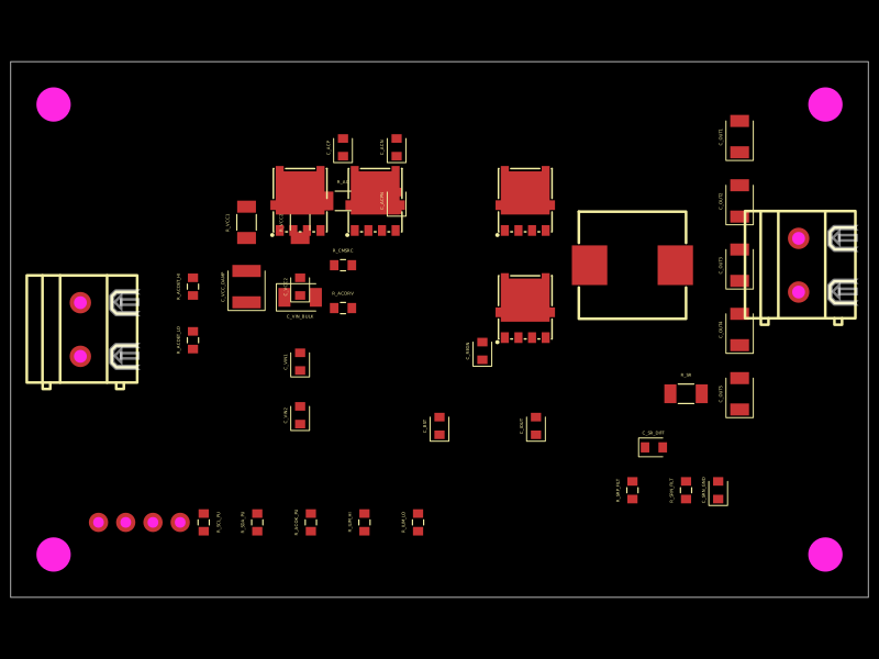 Similar packagejsm/chargerAn 80×50 mm 4S Li-ion charger PCB using a BQ24735 controller, protected 24 V input, MOSFET synchronous buck stage, 4.7 µH inductor, current sensing, filtering, XT30 battery output, and SMBus control interface to deliver up to 16.8 V at 5 A.
 Discover something new0hmX/mt41k512m8da-107-it-p-fanoutThis code defines the physical footprint, routing, and layout configuration for a DDR3 memory module using surface-mount pads, vias, and copper traces on a printed circuit board (PCB).