astra/am3352-sbc
A 4-layer AM3352 single-board computer with 128‑MiB DDR3, PMIC power regulation, USB‑C 5‑V PD input, dual USB host ports, HDMI output with ESD protection, microSD/UART/JTAG interfaces, addressable RGB indicators, and a PWM-driven buzzer.
- Version
- 0.1.19
- License
- unset
- Stars
- 0
design/fabrication-stackup.json
{
  "fabricator": "JLCPCB",
  "nominalBoardThicknessMm": 1.6,
  "stackupCode": "JLC04161H-3313",
  "manufacturerTemplateId": "6381a6960c0a46dba4daf70c97bd5dce",
  "status": "selected; dimensions calculated; copper migration and signoff incomplete",
  "layers": [
    {
      "name": "top",
      "function": "DDR_1V5 reference plane and local component escapes",
      "copperThicknessMm": 0.035
    },
    {
      "material": "3313 RC57%",
      "dielectricThicknessMm": 0.0994,
      "dielectricConstant": 4.1
    },
    {
      "name": "inner1",
      "function": "signals",
      "copperThicknessMm": 0.0152
    },
    {
      "material": "NP-155F core",
      "dielectricThicknessMm": 1.265,
      "dielectricConstant": 4.42
    },
    {
      "name": "inner2",
      "function": "signals",
      "copperThicknessMm": 0.0152
    },
    {
      "material": "3313 RC57%",
      "dielectricThicknessMm": 0.0994,
      "dielectricConstant": 4.1
    },
    {
      "name": "bottom",
      "function": "GND reference plane",
      "copperThicknessMm": 0.035
    }
  ],
  "routingTargets": {
    "singleEnded": {
      "ohms": 50,
      "trackWidthMm": 0.14,
      "calculatorOhms": 49.637857863
    },
    "usb": {
      "ohms": 90,
      "trackWidthMm": 0.1,
      "edgeGapMm": 0.1,
      "calculatorOhms": 90.0694608892
    },
    "ddrClockAndStrobes": {
      "ohms": 100,
      "trackWidthMm": 0.1,
      "edgeGapMm": 0.18,
      "calculatorOhms": 100.921304738
    },
    "hdmi": {
      "ohms": 100,
      "trackWidthMm": 0.1,
      "edgeGapMm": 0.18,
      "calculatorOhms": 100.921304738
    }
  },
  "calculation": {
    "provider": "JLCPCB calculator",
    "referencePlanes": [
      "L1",
      "L4"
    ],
    "model": "OffsetStripline1B1A / DiffOffsetStripline1B1A",
    "report": "references/jlcpcb/inner-signal-impedance-sweep.json",
    "limitations": "Other signal layer is not a plane. Far-side mixed dielectric represented by series-effective permittivity; no solder mask, vias, pads, or plane discontinuities. Manufacturer coupon/engineering approval required."
  },
  "sources": [
    "https://jlcpcb.com/impedance",
    "https://jlcpcb.com/pcb-impedance-calculator",
    "https://jlcpcb.com/api/jlcTools/impedance/selectPageImpedanceDefaultTemplate"
  ],
  "fabricationReady": false,
  "remainingChecks": [
    "Manufacturer must confirm actual four-layer outer-plane / inner-signal impedance coupon and TI +/-5 ohm single-ended tolerance.",
    "Existing DDR copper is 0.10mm, not migrated to 0.14mm single-ended target.",
    "Verify continuous top DDR_1V5 and bottom GND references, return-current stitching and pad/via discontinuities.",
    "Independent native clearance/connectivity, timing, complete supply distribution and SI validation."
  ]
}
Related Packages
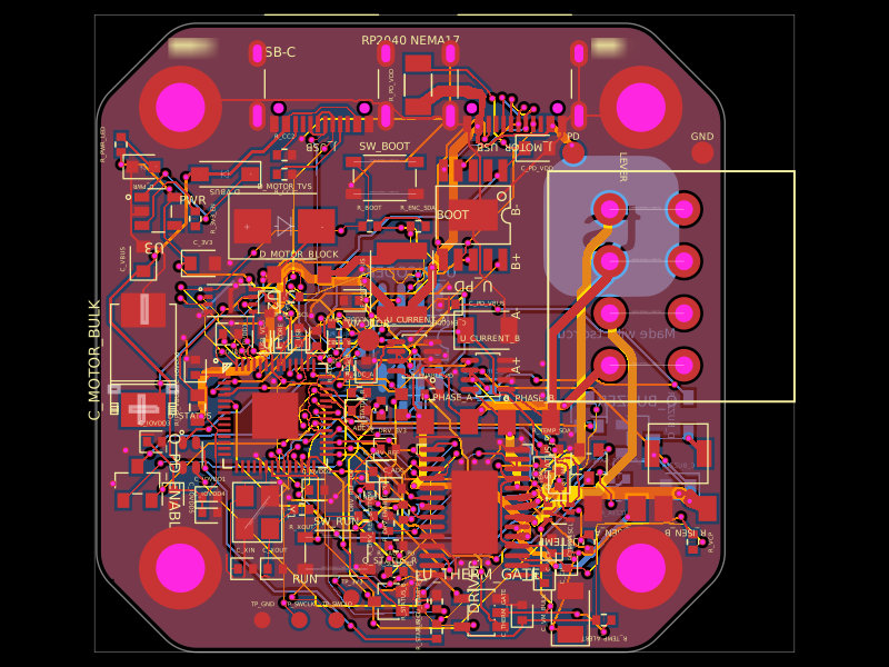 More from this authorastra/nema17-stepper-motor-controller-spring-clamp-rp2040A 4-layer RP2040 controller board that negotiates USB‑C PD motor power and drives a NEMA17 stepper via a DRV8825, with current sensing, thermal shutdown, RGB status LED, buzzer alarm, optional AS5600 encoder, protection/filtering, and test points.
 Similar packageaura/diy-power-delivery-triggerThis hardware design implements a USB Type-C port with supporting power management and signal conditioning components, including a USB-C connector, a FUSB302 USB-C port controller, ESD protection diodes, a buck converter for 3.3V power regulation, an STM32 microcontroller for control and processing, an RGB LED indicator, push button, terminal block connections, and associated filtering and support components.
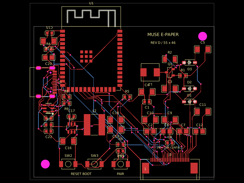 Discover something newmuse/esp32-eink-displayA 55×46 mm two-layer ESP32-S3 e-paper controller board with USB‑C power/programming, buck regulation, FPC display connector, UC8179-style boost/charge-pump circuitry, ESD protection, controls, and routed passive components.