adammlab/smart-pomodoro
This design implements a compact hardware system featuring a USB-C power and ESD protection, a battery charging and load-sharing circuit with TP4056 and P-MOSFET, a 3.3V LDO regulator (ME6211), an ESP32-C3 microcontroller, a 0.96" OLED display with I2C, I2S audio output with MAX98357A amplifier and speaker, a WS2812B RGB LED for visual feedback, and user push buttons, all interconnected with appropriate filtering, decoupling, and mounting hardware.
- Version
- 1.0.4
- License
- unset
- Stars
- 0
index.circuit.tsx
PCB
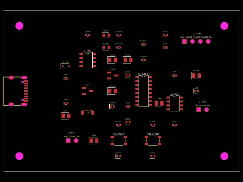
Schematic

import React from "react"

export default () => (
  <board width="76mm" height="52mm" layers={2}>

    {/* =========================================================================
        SECTION 1: USB-C POWER INPUT & ESD PROTECTION (Left Edge)
        ========================================================================= */}
    <schematicsection name="Power_Input" />

    {/* USB-C Receptacle: Facing left board edge */}
    <connector
      name="J_USB"
      standard="usb_c"
      schSectionName="Power_Input"
      schX={-38}
      schY={0}
      pcbX={-33}
      pcbY={0}
      pcbRotation={270}
    />

    {/* ESD TVS Diode on VBUS (5.5V clamp) */}
    <diode
      name="D_TVS"
      footprint="sod323"
      schSectionName="Power_Input"
      schX={-30}
      schY={0}
      pcbX={-18}
      pcbY={8}
    />

    {/* VBUS filter capacitor */}
    <capacitor
      name="C_VBUS"
      capacitance="10uF"
      footprint="0805"
      schSectionName="Power_Input"
      schX={-30}
      schY={4}
      pcbX={-18}
      pcbY={-8}
    />

    {/* CC1 pull-down resistor (5.1k for USB-C 5V detection) */}
    <resistor
      name="R_CC1"
      resistance="5.1k"
      footprint="0402"
      schSectionName="Power_Input"
      schX={-34}
      schY={6}
      pcbX={-18}
      pcbY={4}
    />

    {/* CC2 pull-down resistor */}
    <resistor
      name="R_CC2"
      resistance="5.1k"
      footprint="0402"
      schSectionName="Power_Input"
      schX={-34}
      schY={8}
      pcbX={-18}
      pcbY={-4}
    />

    {/* =========================================================================
        SECTION 2: BATTERY CHARGING (TP4056) & LOAD-SHARING POWER PATH
        ========================================================================= */}
    <schematicsection name="Charging" />

    {/* TP4056 LiPo Charger IC (SOIC-8) */}
    <chip
      name="U_CHG"
      footprint="soic8_p1.27mm"
      schSectionName="Charging"
      schX={-20}
      schY={0}
      pcbX={-11}
      pcbY={10}
      pinLabels={{
        pin1: "TEMP",
        pin2: "PROG",
        pin3: "VSS",
        pin4: "BAT",
        pin5: "STDBY",
        pin6: "CHRG",
        pin7: "VCC",
        pin8: "CE",
      }}
      schPinArrangement={{
        topSide: { pins: ["VCC"], direction: "left-to-right" },
        bottomSide: { pins: ["VSS"], direction: "left-to-right" },
        leftSide: { pins: ["CE", "PROG", "TEMP"], direction: "top-to-bottom" },
        rightSide: { pins: ["BAT", "CHRG", "STDBY"], direction: "top-to-bottom" },
      }}
    />

    {/* Charge current programming resistor (2k = 600mA charge current) */}
    <resistor
      name="R_PROG"
      resistance="2k"
      footprint="0402"
      schSectionName="Charging"
      schX={-24}
      schY={3}
      pcbX={-11}
      pcbY={18}
    />

    {/* Charging status LED (red) */}
    <led
      name="LED_CHG"
      footprint="0603"
      schSectionName="Charging"
      schX={-14}
      schY={3}
      pcbX={-5}
      pcbY={18}
    />

    {/* Charging LED current-limiting resistor */}
    <resistor
      name="R_CHG_LED"
      resistance="1k"
      footprint="0402"
      schSectionName="Charging"
      schX={-14}
      schY={6}
      pcbX={-1}
      pcbY={18}
    />

    {/* Standby (full charge) status LED (green) */}
    <led
      name="LED_FULL"
      footprint="0603"
      schSectionName="Charging"
      schX={-12}
      schY={3}
      pcbX={-5}
      pcbY={14}
    />

    <resistor
      name="R_FULL_LED"
      resistance="1k"
      footprint="0402"
      schSectionName="Charging"
      schX={-12}
      schY={6}
      pcbX={-1}
      pcbY={14}
    />

    {/* Load-Sharing P-MOSFET (AO3401 / SOT-23): Routes battery to system when USB absent */}
    <chip
      name="Q_LS"
      footprint="sot23"
      schSectionName="Charging"
      schX={-8}
      schY={0}
      pcbX={-11}
      pcbY={0}
      pinLabels={{
        pin1: "gate",
        pin2: "source",
        pin3: "drain",
      }}
    />

    {/* Load-Sharing Schottky Diode (1N5819 / SOD-123): Routes USB VBUS directly to system */}
    <diode
      name="D_SCHOTTKY"
      footprint="sod123"
      schSectionName="Charging"
      schX={-8}
      schY={6}
      pcbX={-11}
      pcbY={-7}
    />

    {/* Battery connector (JST PH 2-pin - facing bottom edge) */}
    <connector
      name="J_BAT"
      footprint="pinrow2_p2.54mm"
      schSectionName="Charging"
      schX={-14}
      schY={-6}
      pcbX={-16}
      pcbY={-16}
      pinLabels={{
        pin1: "VBAT_POS",
        pin2: "VBAT_GND",
      }}
    />

    {/* Battery output filter capacitor */}
    <capacitor
      name="C_BAT"
      capacitance="10uF"
      footprint="0805"
      schSectionName="Charging"
      schX={-18}
      schY={-6}
      pcbX={-9}
      pcbY={-16}
    />

    {/* =========================================================================
        SECTION 3: 3.3V LDO VOLTAGE REGULATOR (ME6211)
        ========================================================================= */}
    <schematicsection name="Regulator" />

    {/* ME6211C33 LDO (SOT-23) */}
    <chip
      name="U_LDO"
      footprint="sot23"
      schSectionName="Regulator"
      schX={0}
      schY={0}
      pcbX={-3}
      pcbY={5}
      pinLabels={{
        pin1: "VIN",
        pin2: "VSS",
        pin3: "VOUT",
      }}
      schPinArrangement={{
        leftSide: { pins: ["VIN"], direction: "top-to-bottom" },
        bottomSide: { pins: ["VSS"], direction: "left-to-right" },
        rightSide: { pins: ["VOUT"], direction: "top-to-bottom" },
      }}
    />

    {/* LDO input capacitor */}
    <capacitor
      name="C_LDO_IN"
      capacitance="10uF"
      footprint="0805"
      schSectionName="Regulator"
      schX={-3}
      schY={3}
      pcbX={-3}
      pcbY={10}
    />

    {/* LDO output capacitor */}
    <capacitor
      name="C_LDO_OUT"
      capacitance="10uF"
      footprint="0805"
      schSectionName="Regulator"
      schX={3}
      schY={3}
      pcbX={-3}
      pcbY={0}
    />

    {/* LDO output decoupling */}
    <capacitor
      name="C_LDO_DEC"
      capacitance="100nF"
      footprint="0402"
      schSectionName="Regulator"
      schX={5}
      schY={3}
      pcbX={-3}
      pcbY={-5}
    />

    {/* =========================================================================
        SECTION 4: ESP32-C3 MICROCONTROLLER (Center)
        ========================================================================= */}
    <schematicsection name="MCU" />

    {/* ESP32-C3 MCU (QFN-16) */}
    <chip
      name="U_MCU"
      footprint="soic16_p1.27mm"
      schSectionName="MCU"
      schX={14}
      schY={0}
      pcbX={7}
      pcbY={0}
      pinLabels={{
        pin1: "GND",
        pin2: "3V3",
        pin3: "EN",
        pin4: "IO4",
        pin5: "IO5",
        pin6: "IO6",
        pin7: "IO7",
        pin8: "IO8",
        pin9: "IO9",
        pin10: "IO10",
        pin11: "RX",
        pin12: "TX",
        pin13: "IO18",
        pin14: "IO19",
        pin15: "IO20",
        pin16: "IO21",
      }}
      schPinArrangement={{
        topSide: { pins: ["3V3"], direction: "left-to-right" },
        bottomSide: { pins: ["GND"], direction: "left-to-right" },
        leftSide: {
          pins: ["EN", "IO4", "IO5", "IO6", "IO7", "IO8"],
          direction: "top-to-bottom",
        },
        rightSide: {
          pins: ["IO9", "IO10", "RX", "TX", "IO18", "IO19", "IO20", "IO21"],
          direction: "top-to-bottom",
        },
      }}
    />

    {/* MCU Decoupling Caps */}
    <capacitor
      name="C_MCU1"
      capacitance="100nF"
      footprint="0402"
      schSectionName="MCU"
      schX={8}
      schY={-4}
      pcbX={2}
      pcbY={5}
    />
    <capacitor
      name="C_MCU2"
      capacitance="10uF"
      footprint="0805"
      schSectionName="MCU"
      schX={8}
      schY={-7}
      pcbX={2}
      pcbY={10}
    />

    {/* EN pull-up resistor (10k to 3V3) */}
    <resistor
      name="R_EN"
      resistance="10k"
      footprint="0402"
      schSectionName="MCU"
      schX={8}
      schY={0}
      pcbX={2}
      pcbY={-5}
    />

    {/* EN reset filter cap (100nF to GND) */}
    <capacitor
      name="C_EN"
      capacitance="100nF"
      footprint="0402"
      schSectionName="MCU"
      schX={8}
      schY={2}
      pcbX={2}
      pcbY={-10}
    />

    {/* Battery voltage sense divider */}
    <resistor
      name="R_VDIV_HI"
      resistance="100k"
      footprint="0402"
      schSectionName="MCU"
      schX={22}
      schY={4}
      pcbX={7}
      pcbY={10}
    />
    <resistor
      name="R_VDIV_LO"
      resistance="100k"
      footprint="0402"
      schSectionName="MCU"
      schX={22}
      schY={7}
      pcbX={7}
      pcbY={15}
    />

    {/* =========================================================================
        SECTION 5: DISPLAY (0.96" OLED SSD1306 I2C - Top Edge)
        ========================================================================= */}
    <schematicsection name="Display" />

    {/* 4-Pin OLED Header: facing top edge (y+) */}
    <connector
      name="J_OLED"
      footprint="pinrow4_p2.54mm"
      schSectionName="Display"
      schX={30}
      schY={8}
      pcbX={24}
      pcbY={16}
      pinLabels={{
        pin1: "OLED_GND",
        pin2: "OLED_VCC",
        pin3: "OLED_SCL",
        pin4: "OLED_SDA",
      }}
    />

    {/* I2C pull-up resistors */}
    <resistor
      name="R_SCL"
      resistance="4.7k"
      footprint="0402"
      schSectionName="Display"
      schX={26}
      schY={8}
      pcbX={14}
      pcbY={14}
    />
    <resistor
      name="R_SDA"
      resistance="4.7k"
      footprint="0402"
      schSectionName="Display"
      schX={26}
      schY={11}
      pcbX={14}
      pcbY={18}
    />

    {/* =========================================================================
        SECTION 6: I2S AUDIO (MAX98357A) + SPEAKER (Right Edge)
        ========================================================================= */}
    <schematicsection name="Audio" />

    {/* MAX98357A I2S Class-D Amplifier */}
    <chip
      name="U_AMP"
      footprint="soic8_p1.27mm"
      schSectionName="Audio"
      schX={30}
      schY={-8}
      pcbX={17}
      pcbY={-4}
      pinLabels={{
        pin1: "SD_MODE",
        pin2: "GAIN_SLOT",
        pin3: "GND1",
        pin4: "DIN",
        pin5: "BCLK",
        pin6: "LRCLK",
        pin7: "VDD",
        pin8: "OUTP",
      }}
      schPinArrangement={{
        topSide: { pins: ["VDD"], direction: "left-to-right" },
        bottomSide: { pins: ["GND1"], direction: "left-to-right" },
        leftSide: {
          pins: ["SD_MODE", "GAIN_SLOT", "BCLK", "LRCLK", "DIN"],
          direction: "top-to-bottom",
        },
        rightSide: { pins: ["OUTP"], direction: "top-to-bottom" },
      }}
    />

    {/* Audio amp decoupling */}
    <capacitor
      name="C_AMP"
      capacitance="10uF"
      footprint="0805"
      schSectionName="Audio"
      schX={26}
      schY={-6}
      pcbX={12}
      pcbY={-4}
    />

    {/* Speaker connector: facing right edge (x+) */}
    <connector
      name="J_SPK"
      footprint="pinrow2_p2.54mm"
      schSectionName="Audio"
      schX={36}
      schY={-8}
      pcbX={26}
      pcbY={-6}
      pinLabels={{
        pin1: "SPK_POS",
        pin2: "SPK_NEG",
      }}
    />

    {/* SD_MODE pull-up to enable the amp */}
    <resistor
      name="R_SD"
      resistance="100k"
      footprint="0402"
      schSectionName="Audio"
      schX={26}
      schY={-11}
      pcbX={17}
      pcbY={-11}
    />

    {/* =========================================================================
        SECTION 7: WS2812B RGB LED (BREATHING / ENTRAINMENT)
        ========================================================================= */}
    <schematicsection name="LED_Section" />

    {/* WS2812B Addressable RGB LED */}
    <chip
      name="LED_RGB"
      footprint="0805"
      schSectionName="LED_Section"
      schX={30}
      schY={0}
      pcbX={24}
      pcbY={5}
      pinLabels={{
        pin1: "VDD_LED",
        pin2: "DOUT",
        pin3: "VSS_LED",
        pin4: "DIN_LED",
      }}
    />

    {/* WS2812B data line filter resistor */}
    <resistor
      name="R_WS"
      resistance="330"
      footprint="0402"
      schSectionName="LED_Section"
      schX={26}
      schY={0}
      pcbX={17}
      pcbY={5}
    />

    {/* WS2812B decoupling */}
    <capacitor
      name="C_WS"
      capacitance="100nF"
      footprint="0402"
      schSectionName="LED_Section"
      schX={30}
      schY={3}
      pcbX={24}
      pcbY={0}
    />

    {/* =========================================================================
        SECTION 8: USER INTERFACE (PUSH BUTTONS - Bottom Edge)
        ========================================================================= */}
    <schematicsection name="Buttons" />

    {/* Mode Button */}
    <pushbutton
      name="BTN_MODE"
      footprint="smdpushbutton"
      schSectionName="Buttons"
      schX={4}
      schY={-12}
      pcbX={-1}
      pcbY={-16}
    />

    {/* Start/Stop Button */}
    <pushbutton
      name="BTN_START"
      footprint="smdpushbutton"
      schSectionName="Buttons"
      schX={4}
      schY={-16}
      pcbX={10}
      pcbY={-16}
    />

    {/* Button pull-up resistors */}
    <resistor
      name="R_BTN1"
      resistance="10k"
      footprint="0402"
      schSectionName="Buttons"
      schX={0}
      schY={-12}
      pcbX={-1}
      pcbY={-11}
    />
    <resistor
      name="R_BTN2"
      resistance="10k"
      footprint="0402"
      schSectionName="Buttons"
      schX={0}
      schY={-16}
      pcbX={10}
      pcbY={-11}
    />

    {/* Button debounce caps */}
    <capacitor
      name="C_BTN1"
      capacitance="100nF"
      footprint="0402"
      schSectionName="Buttons"
      schX={2}
      schY={-14}
      pcbX={-1}
      pcbY={-21}
    />
    <capacitor
      name="C_BTN2"
      capacitance="100nF"
      footprint="0402"
      schSectionName="Buttons"
      schX={2}
      schY={-18}
      pcbX={10}
      pcbY={-21}
    />

    {/* =========================================================================
        SECTION 9: MOUNTING HOLES (Corners)
        ========================================================================= */}
    <hole name="MH1" diameter="2.5mm" pcbX={-33} pcbY={-21} />
    <hole name="MH2" diameter="2.5mm" pcbX={33} pcbY={-21} />
    <hole name="MH3" diameter="2.5mm" pcbX={-33} pcbY={21} />
    <hole name="MH4" diameter="2.5mm" pcbX={33} pcbY={21} />

    {/* =========================================================================
        TRACES & NETS: POWER DISTRIBUTION
        ========================================================================= */}

    {/* --- USB VBUS Net --- */}
    <trace from=".J_USB > .VBUS1" to="net.VBUS" />
    <trace from=".J_USB > .VBUS2" to="net.VBUS" />
    <trace from=".D_TVS > .pin1" to="net.VBUS" />
    <trace from=".D_TVS > .pin2" to="net.GND" />
    <trace from=".C_VBUS > .pin1" to="net.VBUS" />
    <trace from=".C_VBUS > .pin2" to="net.GND" />

    {/* USB-C CC pull-downs for 5V detection */}
    <trace from=".J_USB > .CC1" to=".R_CC1 > .pin1" />
    <trace from=".R_CC1 > .pin2" to="net.GND" />
    <trace from=".J_USB > .CC2" to=".R_CC2 > .pin1" />
    <trace from=".R_CC2 > .pin2" to="net.GND" />

    {/* USB GND */}
    <trace from=".J_USB > .GND1" to="net.GND" />
    <trace from=".J_USB > .GND2" to="net.GND" />

    {/* --- TP4056 Charger --- */}
    <trace from=".U_CHG > .VCC" to="net.VBUS" />
    <trace from=".U_CHG > .VSS" to="net.GND" />
    <trace from=".U_CHG > .CE" to="net.VBUS" />
    <trace from=".U_CHG > .PROG" to=".R_PROG > .pin1" />
    <trace from=".R_PROG > .pin2" to="net.GND" />
    <trace from=".U_CHG > .TEMP" to="net.GND" />
    <trace from=".U_CHG > .BAT" to="net.VBAT" />

    {/* Charging status LEDs */}
    <trace from=".U_CHG > .CHRG" to=".LED_CHG > .pin1" />
    <trace from=".LED_CHG > .pin2" to=".R_CHG_LED > .pin1" />
    <trace from=".R_CHG_LED > .pin2" to="net.GND" />

    <trace from=".U_CHG > .STDBY" to=".LED_FULL > .pin1" />
    <trace from=".LED_FULL > .pin2" to=".R_FULL_LED > .pin1" />
    <trace from=".R_FULL_LED > .pin2" to="net.GND" />

    {/* --- Battery Connector --- */}
    <trace from=".J_BAT > .VBAT_POS" to="net.VBAT" />
    <trace from=".J_BAT > .VBAT_GND" to="net.GND" />
    <trace from=".C_BAT > .pin1" to="net.VBAT" />
    <trace from=".C_BAT > .pin2" to="net.GND" />

    {/* --- Load-Sharing Power Path --- */}
    {/* Schottky diode: USB VBUS -> V_SYS (direct power when USB present) */}
    <trace from=".D_SCHOTTKY > .pin1" to="net.VBUS" />
    <trace from=".D_SCHOTTKY > .pin2" to="net.V_SYS" />

    {/* P-MOSFET: Battery -> V_SYS (backup when USB absent) */}
    <trace from=".Q_LS > .gate" to="net.VBUS" />
    <trace from=".Q_LS > .source" to="net.VBAT" />
    <trace from=".Q_LS > .drain" to="net.V_SYS" />

    {/* --- LDO Regulator: V_SYS -> 3.3V --- */}
    <trace from=".U_LDO > .VIN" to="net.V_SYS" />
    <trace from=".U_LDO > .VSS" to="net.GND" />
    <trace from=".U_LDO > .VOUT" to="net.V3_3" />
    <trace from=".C_LDO_IN > .pin1" to="net.V_SYS" />
    <trace from=".C_LDO_IN > .pin2" to="net.GND" />
    <trace from=".C_LDO_OUT > .pin1" to="net.V3_3" />
    <trace from=".C_LDO_OUT > .pin2" to="net.GND" />
    <trace from=".C_LDO_DEC > .pin1" to="net.V3_3" />
    <trace from=".C_LDO_DEC > .pin2" to="net.GND" />

    {/* =========================================================================
        TRACES & NETS: MCU POWER & ENABLE
        ========================================================================= */}
    <trace from=".U_MCU > .3V3" to="net.V3_3" />
    <trace from=".U_MCU > .GND" to="net.GND" />
    <trace from=".C_MCU1 > .pin1" to="net.V3_3" />
    <trace from=".C_MCU1 > .pin2" to="net.GND" />
    <trace from=".C_MCU2 > .pin1" to="net.V3_3" />
    <trace from=".C_MCU2 > .pin2" to="net.GND" />

    {/* EN pull-up and filter */}
    <trace from=".U_MCU > .EN" to=".R_EN > .pin1" />
    <trace from=".R_EN > .pin2" to="net.V3_3" />
    <trace from=".U_MCU > .EN" to=".C_EN > .pin1" />
    <trace from=".C_EN > .pin2" to="net.GND" />

    {/* Battery voltage sense divider (VBAT -> 100k -> ADC -> 100k -> GND) */}
    <trace from=".R_VDIV_HI > .pin1" to="net.VBAT" />
    <trace from=".R_VDIV_HI > .pin2" to=".U_MCU > .IO4" />
    <trace from=".R_VDIV_LO > .pin1" to=".U_MCU > .IO4" />
    <trace from=".R_VDIV_LO > .pin2" to="net.GND" />

    {/* =========================================================================
        TRACES & NETS: I2C DISPLAY
        ========================================================================= */}
    <trace from=".J_OLED > .OLED_GND" to="net.GND" />
    <trace from=".J_OLED > .OLED_VCC" to="net.V3_3" />
    <trace from=".J_OLED > .OLED_SCL" to=".U_MCU > .IO5" />
    <trace from=".J_OLED > .OLED_SDA" to=".U_MCU > .IO6" />

    {/* I2C pull-ups to 3.3V */}
    <trace from=".R_SCL > .pin1" to="net.V3_3" />
    <trace from=".R_SCL > .pin2" to=".U_MCU > .IO5" />
    <trace from=".R_SDA > .pin1" to="net.V3_3" />
    <trace from=".R_SDA > .pin2" to=".U_MCU > .IO6" />

    {/* =========================================================================
        TRACES & NETS: I2S AUDIO
        ========================================================================= */}
    <trace from=".U_AMP > .VDD" to="net.V3_3" />
    <trace from=".U_AMP > .GND1" to="net.GND" />
    <trace from=".C_AMP > .pin1" to="net.V3_3" />
    <trace from=".C_AMP > .pin2" to="net.GND" />

    {/* I2S signals from MCU to Audio Amp */}
    <trace from=".U_MCU > .IO7" to=".U_AMP > .DIN" />
    <trace from=".U_MCU > .IO8" to=".U_AMP > .BCLK" />
    <trace from=".U_MCU > .IO9" to=".U_AMP > .LRCLK" />

    {/* SD_MODE enable: pull-up to VCC (always on) */}
    <trace from=".U_AMP > .SD_MODE" to=".R_SD > .pin1" />
    <trace from=".R_SD > .pin2" to="net.V3_3" />

    {/* GAIN_SLOT: tie to GND for 9dB gain (default) */}
    <trace from=".U_AMP > .GAIN_SLOT" to="net.GND" />

    {/* Speaker output */}
    <trace from=".U_AMP > .OUTP" to=".J_SPK > .SPK_POS" />
    <trace from=".J_SPK > .SPK_NEG" to="net.GND" />

    {/* =========================================================================
        TRACES & NETS: WS2812B RGB LED
        ========================================================================= */}
    <trace from=".LED_RGB > .VDD_LED" to="net.V3_3" />
    <trace from=".LED_RGB > .VSS_LED" to="net.GND" />
    <trace from=".C_WS > .pin1" to="net.V3_3" />
    <trace from=".C_WS > .pin2" to="net.GND" />

    {/* Data line: MCU IO10 -> 330Ω -> WS2812B DIN */}
    <trace from=".U_MCU > .IO10" to=".R_WS > .pin1" />
    <trace from=".R_WS > .pin2" to=".LED_RGB > .DIN_LED" />

    {/* =========================================================================
        TRACES & NETS: BUTTONS
        ========================================================================= */}
    {/* Button 1 (Mode): IO18, active low with pull-up */}
    <trace from=".R_BTN1 > .pin1" to="net.V3_3" />
    <trace from=".R_BTN1 > .pin2" to=".U_MCU > .IO18" />
    <trace from=".BTN_MODE > .pin1" to=".U_MCU > .IO18" />
    <trace from=".BTN_MODE > .pin2" to="net.GND" />
    <trace from=".C_BTN1 > .pin1" to=".U_MCU > .IO18" />
    <trace from=".C_BTN1 > .pin2" to="net.GND" />

    {/* Button 2 (Start/Stop): IO19, active low with pull-up */}
    <trace from=".R_BTN2 > .pin1" to="net.V3_3" />
    <trace from=".R_BTN2 > .pin2" to=".U_MCU > .IO19" />
    <trace from=".BTN_START > .pin1" to=".U_MCU > .IO19" />
    <trace from=".BTN_START > .pin2" to="net.GND" />
    <trace from=".C_BTN2 > .pin1" to=".U_MCU > .IO19" />
    <trace from=".C_BTN2 > .pin2" to="net.GND" />

  </board>
)