abse/wifi-smart-switch
The AO3400A component models a small N-channel MOSFET in a SOT-23 package with drain, gate, and source pins, used for switching or amplification in electronic circuits.
- Version
- 1.0.29
- License
- unset
- Stars
- 0
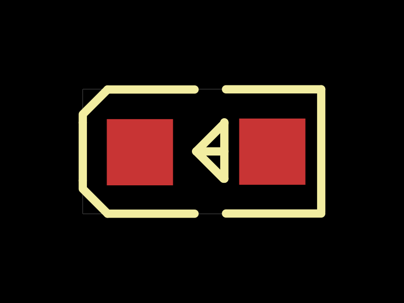
imports/SS14/SS14.tsx
import objPath from "./SS14.obj"
import type { DiodeProps } from "@tscircuit/props"

const pinLabels = {
  pin1: ["cathode","neg"],
  pin2: ["anode","pos"]
} as const

export const SS14 = (props: DiodeProps) => {
  const { name = "D1", ...restProps } = props

  return (
    <diode
      name={name}
      pinLabels={pinLabels}
      supplierPartNumbers={{
  "jlcpcb": [
    "C2480"
  ]
}}
      manufacturerPartNumber="SS14"
      footprint={
        <footprint>
          <smtpad
            portHints={["pin1"]}
            pcbX="-1.96495mm"
            pcbY="0mm"
            width="1.52mm"
            height="1.68mm"
            shape="rect"
          />
          <smtpad
            portHints={["pin2"]}
            pcbX="1.96495mm"
            pcbY="0mm"
            width="1.52mm"
            height="1.68mm"
            shape="rect"
          />
          <silkscreenpath route={[
            { x: -1.1, y: -0.9 },
            { x: 1.1, y: -0.9 },
            { x: 1.1, y: 0.9 },
            { x: -1.1, y: 0.9 },
            { x: -1.1, y: -0.9 },
          ]} />
          <silkscreenpath route={[
            { x: -0.75, y: -0.9 },
            { x: -0.75, y: 0.9 },
          ]} />
          <fabricationnotetext text="-" pcbX="-1.96495mm" pcbY="-1.35mm" fontSize="0.7mm" layer="top" />
          <fabricationnotetext text="+" pcbX="1.96495mm" pcbY="-1.35mm" fontSize="0.7mm" layer="top" />
          <silkscreentext text="{NAME}" pcbX="0mm" pcbY="1.45mm" fontSize="0.8mm" />
        </footprint>
      }
      cadModel={{
        objUrl: objPath,
        pcbRotationOffset: 0,
        modelOriginPosition: { x: 0, y: -0.000012699999956566899, z: -1.05 },
      }}
      {...restProps}
    />
  )
}
Related Packages
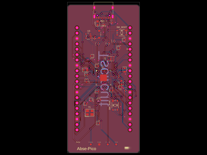 More from this authorabse/abse-picoThis code defines 3D models and footprints for various electronic components—such as voltage regulators, microcontrollers, and memory chips—highlighting their physical pin configurations, mounting pads, and visual identifiers for PCB design.
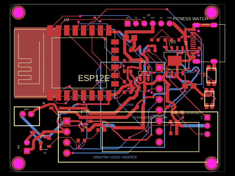 Similar packageimrishabh18/fitness_watchThis code defines a React component representing an AO3400A SOT-23P surface-mount N-channel MOSFET with three pins labeled Gate (G), Source (S), and Drain (D), including electrical and physical pin configurations, schematic symbol, and associated 3D model.
 Discover something newseveibar/red-ledGenerated from JLCPCB part number C965799