abse/smart-ring-flex
A tscircuit package created by abse.
- Version
- 0.0.24
- License
- unset
- Stars
- 0
firmware/onboard-programmer/upstream/src/gpio.h
// ===================================================================================
// Basic GPIO, PWM and ADC Functions for CH551, CH552 and CH554               * v1.5 *
// ===================================================================================
//
// Pins must be defined as P10, P11, P12, etc. - e.g.:
// #define PIN_LED P33      // LED on pin P3.3
//
// Functions available:
// --------------------
// PIN_input(PIN)           set PIN as INPUT (high impedance, no pullup)
// PIN_input_PU(PIN)        set PIN as INPUT with internal PULLUP
// PIN_output(PIN)          set PIN as OUTPUT (push-pull)
// PIN_output_OD(PIN)       set PIN as OUTPUT (open-drain)
//
// PIN_low(PIN)             set PIN output value to LOW
// PIN_high(PIN)            set PIN output value to HIGH
// PIN_toggle(PIN)          TOGGLE PIN output value
// PIN_read(PIN)            read PIN input value
// PIN_write(PIN, val)      write PIN output value (0 = LOW / 1 = HIGH)
//
// PIN_asm(PIN)             convert PIN for inline assembly: setb PIN_asm(PIN_LED)
// PIN_set(PIN)             convert PIN for direct manipulation: PIN_set(PIN_LED) = 1;
//
// PIN_WAKE_enable(PIN)     enable wake-up from sleep by PIN low (P13, P14, P15 only)
// PIN_WAKE_disable(PIN)    disable wake-up from sleep by PIN low
//
// PWM_start(PIN)           start PWM output on PIN, can be (P15 or P30) and (P34 or P31)
// PWM_stop(PIN)            stop PWM output on PIN
// PWM_write(PIN, val)      set PWM output active level duty cycle on PIN
//
// PWM_pol_normal(PIN)      set normal PWM polarity on PIN (default low and active high)
// PWM_pol_reverse(PIN)     set reverse PWM polarity on PIN (default high and active low)
// PWM_set_freq(FREQ)       set global PWM frequency (in Hertz)
//
// ADC_enable()             enable ADC
// ADC_disable()            disable ADC
// ADC_fast()               set ADC fast mode ( 96 clock cycles per sample, less accurate)
// ADC_slow()               set ADC slow mode (384 clock cycles per sample, more accurate)
// ADC_input(PIN)           set ADC input pin (P11, P14, P15, P32 only)
// ADC_read()               sample and read ADC value (0..255)
//
// CMP_enable()             enable comparator
// CMP_disable()            disable comparator
// CMP_positive(PIN)        set CMP non-inverting input pin (P11, P14, P15, P32 only)
// CMP_negative(PIN)        set CMP inverting input pin (P14, P32 only)
// CMP_read()               read CMP output (0: pos < neg, 1: pos > neg)
//
// Notes:
// ------
// Pins used for PWM should be set as OUTPUT beforehand.
// Pins used for ADC or CMP must have been set as INPUT (high impedance) beforehand.
//
// 2022 by Stefan Wagner:   https://github.com/wagiminator

#pragma once
#include <stdint.h>
#include "ch554.h"

// ===================================================================================
// Enumerate pin designators (use these designators to define pins)
// ===================================================================================

enum{P10, P11, P12, P13, P14, P15, P16, P17, P30, P31, P32, P33, P34, P35, P36, P37};

// ===================================================================================
// Helper Defines (these are for internal use only)
// ===================================================================================

// Define pins for direct bit manipulation
SBIT(PP10, 0x90, 0);
SBIT(PP11, 0x90, 1);
SBIT(PP12, 0x90, 2);
SBIT(PP13, 0x90, 3);
SBIT(PP14, 0x90, 4);
SBIT(PP15, 0x90, 5);
SBIT(PP16, 0x90, 6);
SBIT(PP17, 0x90, 7);
SBIT(PP30, 0xB0, 0);
SBIT(PP31, 0xB0, 1);
SBIT(PP32, 0xB0, 2);
SBIT(PP33, 0xB0, 3);
SBIT(PP34, 0xB0, 4);
SBIT(PP35, 0xB0, 5);
SBIT(PP36, 0xB0, 6);
SBIT(PP37, 0xB0, 7);

// 2nd-stage glue defines
#define PIN_h_a(PIN) _P##PIN
#define PIN_h_s(PIN) P##PIN

#define PORT_h_i(PORT, PIN)       (P##PORT##_DIR_PU &= ~(1<<PIN), P##PORT##_MOD_OC &= ~(1<<PIN))
#define PORT_h_iP(PORT, PIN)      (P##PORT##_MOD_OC |=  (1<<PIN), P##PORT##_DIR_PU |=  (1<<PIN))
#define PORT_h_o(PORT, PIN)       (P##PORT##_MOD_OC &= ~(1<<PIN), P##PORT##_DIR_PU |=  (1<<PIN))
#define PORT_h_oO(PORT, PIN)      (P##PORT##_MOD_OC |=  (1<<PIN), P##PORT##_DIR_PU &= ~(1<<PIN))

#define PORT_h_l(PORT, PIN)       PP##PORT##PIN = 0
#define PORT_h_h(PORT, PIN)       PP##PORT##PIN = 1
#define PORT_h_t(PORT, PIN)       PP##PORT##PIN = !PP##PORT##PIN
#define PORT_h_r(PORT, PIN)       (PP##PORT##PIN)
#define PORT_h_w(PORT,PIN,val)    PP##PORT##PIN = val

// ===================================================================================
// Set pin as INPUT (high impedance, no pullup)
// ===================================================================================
#define PIN_input(PIN) \
  ((PIN>=P10)&&(PIN<=P17) ? (P1_DIR_PU &= ~(1<<(PIN&7)), P1_MOD_OC &= ~(1<<(PIN&7))) : \
  ((PIN>=P30)&&(PIN<=P37) ? (P3_DIR_PU &= ~(1<<(PIN&7)), P3_MOD_OC &= ~(1<<(PIN&7))) : \
(0)))

#define PIN_input_HI    PIN_input
#define PIN_input_FL    PIN_input

// ===================================================================================
// Set pin as INPUT with internal PULLUP resistor (also open-drain output,
// when output changes from LOW to HIGH, it will drive HIGH for 2 clock cycles)
// ===================================================================================
#define PIN_input_PU(PIN) \
  ((PIN>=P10)&&(PIN<=P17) ? (P1_MOD_OC |= (1<<(PIN&7)), P1_DIR_PU |= (1<<(PIN&7))) : \
  ((PIN>=P30)&&(PIN<=P37) ? (P3_MOD_OC |= (1<<(PIN&7)), P3_DIR_PU |= (1<<(PIN&7))) : \
(0)))

// ===================================================================================
// Set pin as OUTPUT (push-pull)
// ===================================================================================
#define PIN_output(PIN) \
  ((PIN>=P10)&&(PIN<=P17) ? (P1_MOD_OC &= ~(1<<(PIN&7)), P1_DIR_PU |= (1<<(PIN&7))) : \
  ((PIN>=P30)&&(PIN<=P37) ? (P3_MOD_OC &= ~(1<<(PIN&7)), P3_DIR_PU |= (1<<(PIN&7))) : \
(0)))

#define PIN_output_PP   PIN_output

// ===================================================================================
// Set pin as OPEN-DRAIN OUTPUT (also high-impedance input, no pullup)
// ===================================================================================
#define PIN_output_OD(PIN) \
  ((PIN>=P10)&&(PIN<=P17) ? (P1_MOD_OC |= (1<<(PIN&7)), P1_DIR_PU &= ~(1<<(PIN&7))) : \
  ((PIN>=P30)&&(PIN<=P37) ? (P3_MOD_OC |= (1<<(PIN&7)), P3_DIR_PU &= ~(1<<(PIN&7))) : \
(0)))

// ===================================================================================
// Pin manipulation macros
// ===================================================================================
#define PIN_low(PIN)          PIN_h_s(PIN) = 0              // set pin to LOW
#define PIN_high(PIN)         PIN_h_s(PIN) = 1              // set pin to HIGH
#define PIN_toggle(PIN)       PIN_h_s(PIN) = !PIN_h_s(PIN)  // TOGGLE pin
#define PIN_read(PIN)         (PIN_h_s(PIN))                // READ pin
#define PIN_write(PIN, val)   PIN_h_s(PIN) = val            // WRITE pin value

// ===================================================================================
// (PORT, PIN) manipulation macros
// ===================================================================================
#define PORT_input(PORT, PIN)     PORT_h_i(PORT, PIN)       // set pin as INPUT
#define PORT_input_PU(PORT, PIN)  PORT_h_iP(PORT, PIN)      // set pin as INPUT PULLUP
#define PORT_output(PORT, PIN)    PORT_h_o(PORT, PIN)       // set pin as OUTPUT
#define PORT_output_OD(PORT, PIN) PORT_h_oO(PORT, PIN)      // set pin as OUTPUT OPEN-DRAIN

#define PORT_low(PORT, PIN)       PORT_h_l(PORT, PIN)       // set pin to LOW
#define PORT_high(PORT, PIN)      PORT_h_h(PORT, PIN)       // set pin to HIGH
#define PORT_toggle(PORT, PIN)    PORT_h_t(PORT, PIN)       // TOGGLE pin
#define PORT_read(PORT, PIN)      PORT_h_r(PORT, PIN)       // READ pin
#define PORT_write(PORT,PIN,val)  PORT_h_w(PORT, PIN, val)  // WRITE pin value

// ===================================================================================
// Convert pin for inline assembly and direct manipulation
// ===================================================================================
#define PIN_asm(PIN)        PIN_h_a(PIN)
#define PIN_set(PIN)        PIN_h_s(PIN)

// ===================================================================================
// Enable/disable WAKE-up from sleep by pin LOW (P13, P14, P15 only)
// ===================================================================================
#define WAKE_PIN_enable(PIN) \
  ((PIN == P13) ? (WAKE_CTRL |= bWAK_P1_3_LO) : \
  ((PIN == P14) ? (WAKE_CTRL |= bWAK_P1_4_LO) : \
  ((PIN == P15) ? (WAKE_CTRL |= bWAK_P1_5_LO) : \
(0)))))

#define WAKE_PIN_disable(PIN) \
  ((PIN == P13) ? (WAKE_CTRL &= ~bWAK_P1_3_LO) : \
  ((PIN == P14) ? (WAKE_CTRL &= ~bWAK_P1_4_LO) : \
  ((PIN == P15) ? (WAKE_CTRL &= ~bWAK_P1_5_LO) : \
(0)))))

// ===================================================================================
// Start PWM on pin, must be a PWM-capable pin: (P15 or P30) and (P34 or P31)
// ===================================================================================
#define PWM_start(PIN) \
  ((PIN == P15) ? (PWM_CTRL &= ~bPWM_CLR_ALL, PIN_FUNC &= ~bPWM1_PIN_X, PWM_CTRL |= bPWM1_OUT_EN) : \
  ((PIN == P34) ? (PWM_CTRL &= ~bPWM_CLR_ALL, PIN_FUNC &= ~bPWM2_PIN_X, PWM_CTRL |= bPWM2_OUT_EN) : \
  ((PIN == P30) ? (PWM_CTRL &= ~bPWM_CLR_ALL, PIN_FUNC |=  bPWM1_PIN_X, PWM_CTRL |= bPWM1_OUT_EN) : \
  ((PIN == P31) ? (PWM_CTRL &= ~bPWM_CLR_ALL, PIN_FUNC |=  bPWM2_PIN_X, PWM_CTRL |= bPWM2_OUT_EN) : \
(0)))))

// ===================================================================================
// Set PWM output active level duty cycle on pin
// ===================================================================================
#define PWM_write(PIN, val) \
  ((PIN == P15) ? (PWM_DATA1 = val) : \
  ((PIN == P34) ? (PWM_DATA2 = val) : \
  ((PIN == P30) ? (PWM_DATA1 = val) : \
  ((PIN == P31) ? (PWM_DATA2 = val) : \
(0)))))

// ===================================================================================
// Stop PWM on pin
// ===================================================================================
#define PWM_stop(PIN) \
  ((PIN == P15) ? (PWM_CTRL &= ~bPWM1_OUT_EN) : \
  ((PIN == P34) ? (PWM_CTRL &= ~bPWM2_OUT_EN) : \
  ((PIN == P30) ? (PWM_CTRL &= ~bPWM1_OUT_EN) : \
  ((PIN == P31) ? (PWM_CTRL &= ~bPWM2_OUT_EN) : \
(0)))))

// ===================================================================================
// Set normal PWM polarity on pin (default low and active high)
// ===================================================================================
#define PWM_pol_normal(PIN) \
  ((PIN == P15) ? (PWM_CTRL &= ~bPWM1_POLAR) : \
  ((PIN == P34) ? (PWM_CTRL &= ~bPWM2_POLAR) : \
  ((PIN == P30) ? (PWM_CTRL &= ~bPWM1_POLAR) : \
  ((PIN == P31) ? (PWM_CTRL &= ~bPWM2_POLAR) : \
(0)))))

// ===================================================================================
// Set reverse PWM polarity on pin (default high and active low)
// ===================================================================================
#define PWM_pol_reverse(PIN) \
  ((PIN == P15) ? (PWM_CTRL |= bPWM1_POLAR) : \
  ((PIN == P34) ? (PWM_CTRL |= bPWM2_POLAR) : \
  ((PIN == P30) ? (PWM_CTRL |= bPWM1_POLAR) : \
  ((PIN == P31) ? (PWM_CTRL |= bPWM2_POLAR) : \
(0)))))

// ===================================================================================
// Set global PWM frequency (in Hertz, range: F_CPU/65536 - F_CPU/256)
// ===================================================================================
#define PWM_set_freq(FREQ) \
  (((FREQ) >= F_CPU / 256) ? (PWM_CK_SE = 0)              : \
  (((F_CPU / 256 / (FREQ) - 1) > 255) ? (PWM_CK_SE = 255) : \
  (PWM_CK_SE = (uint8_t)(F_CPU / 256 / (FREQ) - 1))         \
))

// ===================================================================================
// Pin to ADC channel conversion (P11, P14, P15, P32 only)
// ===================================================================================
#define ADC_channel(PIN) \
  ((PIN == P11) ? (0) : \
  ((PIN == P14) ? (1) : \
  ((PIN == P15) ? (2) : \
  ((PIN == P32) ? (3) : \
(0)))))

// ===================================================================================
// ADC functions (P11, P14, P15, P32 only)
// ===================================================================================
#define ADC_enable()    ADC_CFG |=  bADC_EN
#define ADC_disable()   ADC_CFG &= ~bADC_EN
#define ADC_fast()      ADC_CFG |=  bADC_CLK
#define ADC_slow()      ADC_CFG &= ~bADC_CLK

#define ADC_input(PIN) \
  ((PIN == P11) ? (ADC_CHAN1 = 0, ADC_CHAN0 = 0) : \
  ((PIN == P14) ? (ADC_CHAN1 = 0, ADC_CHAN0 = 1) : \
  ((PIN == P15) ? (ADC_CHAN1 = 1, ADC_CHAN0 = 0) : \
  ((PIN == P32) ? (ADC_CHAN1 = 1, ADC_CHAN0 = 1) : \
(0)))))

inline uint8_t ADC_read(void) {
  ADC_START = 1;
  while(ADC_START);
  return ADC_DATA;
}

// ===================================================================================
// Pin to comparator inverting input conversion (P14, P32 only)
// ===================================================================================
#define CMP_channel(PIN) \
  ((PIN == P14) ? (0) : \
  ((PIN == P32) ? (1) : \
(0)))

// ===================================================================================
// Comparator functions (positive: P11, P14, P15, P32, negative: P14, P32 only)
// ===================================================================================
#define CMP_enable()    ADC_CFG |=  bCMP_EN
#define CMP_disable()   ADC_CFG &= ~bCMP_EN
#define CMP_read()      (CMPO)

#define CMP_positive(PIN)   ADC_input(PIN)
#define CMP_negative(PIN) \
  ((PIN == P14) ? (CMP_CHAN = 0) : \
  ((PIN == P32) ? (CMP_CHAN = 1) : \
(0)))
Related Packages
 More from this authorabse/museair-usb-assemblyA mechanically secured SEN62 sensor carrier integrates a JLC PCB, bound GH6 harness, USB power cable, fasteners, retention hardware, and protective outer enclosure.
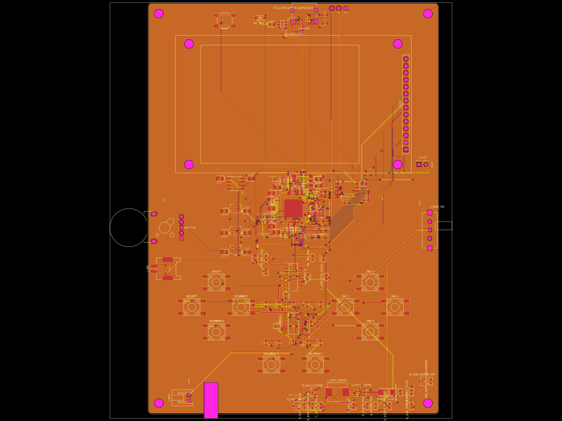 Discover something newShiboSoftwareDev/f1c100s-linux-gameboyRestores PCB assembly metadata by assigning part numbers, managing 3D CAD models and orientations, removing test-point bodies, and validating top-side SMT solder-paste features.