abse/museair-usb
USB-C–powered ESP32-C3 controller board with AP63203 buck conversion, AP2112K 3.3V regulation, I²C SEN62 sensor interface, status LED, buttons, UART/I²C headers, and extensive decoupling.
- Version
- 0.5.7
- License
- unset
- Stars
- 0
scripts/prepare-kicad.py
"""Repair known tscircuit 0.0.2444 KiCad export metadata defects.

Usage: KiCad's bundled Python prepare-kicad.py circuit.json raw.kicad_pcb output.kicad_pcb
Source-pad geometry and net assignments are retained. Two free routing
vertices from earlier routes have guarded clearance corrections; native DRC
checks this release, which does not require those old corrections.
KiCad refills the ground
zones against the exact pads after restoring duplicate-pin net assignments.
The plot origin is the board's lower-left corner, shared with the assembly CPL.
"""
import json, sys, os, math
import wx
import pcbnew as pcb
# Initialize the wx runtime used by KiCad native I/O.
wx_app = wx.App(False)

source, raw_path, output = sys.argv[1:4]
report_path = sys.argv[4] if len(sys.argv)>4 else None
cs = json.load(open(source))
b = pcb.LoadBoard(raw_path)
# Keep removed objects alive until process exit: KiCad 10 SWIG destructors
# can invalidate other native wrapper types when collected mid-export.
removed_native_items = []
footprints = list(b.GetFootprints())
sc = {x['source_component_id']: x for x in cs if x['type'] == 'source_component'}
net_by_key = {x['subcircuit_connectivity_map_key']: x['name'] for x in cs if x['type'] == 'source_net'}
pad_net = {}
for p in (x for x in cs if x['type'] == 'source_port'):
    if p['source_component_id'] not in sc or 'pin_number' not in p:
        continue
    name = sc[p['source_component_id']]['name']
    net_name = net_by_key.get(p.get('subcircuit_connectivity_map_key'))
    if net_name:
        pad_net[(name, str(p['pin_number']))] = net_name
repairs = {'pad_net_assignments': 0, 'two_point_courtyard_polygons': 0, 'duplicate_copper_items': 0}
for f in footprints:
    for pad in f.Pads():
        name = pad_net.get((f.GetReference(), pad.GetNumber()))
        if name and pad.GetNetname() != name:
            pad.SetNet(b.FindNet(name))
            repairs['pad_net_assignments'] += 1
        if f.GetReference() in ('J4','J5'):
            layers=pad.GetLayerSet();layers.RemoveLayer(pcb.F_Paste);layers.RemoveLayer(pcb.B_Paste);pad.SetLayerSet(layers)
    for g in list(f.GraphicalItems()):
        if g.GetLayer() in (pcb.F_CrtYd, pcb.B_CrtYd) and g.GetShape() == pcb.SHAPE_T_POLY:
            points = list(g.GetPolyShape().Outline(0).CPoints())
            if len(points) == 2:
                g.SetShape(pcb.SHAPE_T_SEGMENT)
                g.SetStart(points[0]); g.SetEnd(points[1])
                repairs['two_point_courtyard_polygons'] += 1
seen = set()
for t in list(b.GetTracks()):
    if isinstance(t, pcb.PCB_VIA):
        key = ('via', t.GetNetCode(), t.GetPosition().x, t.GetPosition().y, t.GetWidth(pcb.F_Cu), t.GetDrillValue())
    else:
        ends = sorted([(t.GetStart().x, t.GetStart().y), (t.GetEnd().x, t.GetEnd().y)])
        key = ('track', t.GetNetCode(), t.GetLayer(), tuple(ends), t.GetWidth())
    if key in seen:
        removed_native_items.append(t); b.Remove(t); repairs['duplicate_copper_items'] += 1
    else:
        seen.add(key)
# The autorouter sometimes places two same-net vias so close that their drill
# holes violate 0.2 mm spacing. Retain one hole and join the old endpoints on
# both layers. The short links lie inside the two original overlapping lands.
repairs['same_net_vias_coalesced'] = 0
vias = [t for t in b.GetTracks() if isinstance(t, pcb.PCB_VIA)]
for i, master in enumerate(vias):
    if master is None: continue
    for j in range(i+1,len(vias)):
        other = vias[j]
        if other is None or master.GetNetCode()!=other.GetNetCode(): continue
        a,c=master.GetPosition(),other.GetPosition()
        distance=math.hypot(a.x-c.x,a.y-c.y)
        min_distance=(master.GetDrillValue()+other.GetDrillValue())/2+pcb.FromMM(0.2)
        if distance < min_distance:
            # Restrict this repair to overlapping same-size 0.6 mm lands.
            assert master.GetWidth(pcb.F_Cu)==other.GetWidth(pcb.F_Cu)==pcb.FromMM(0.6)
            assert distance < pcb.FromMM(0.5)
            for layer in (pcb.F_Cu,pcb.B_Cu):
                link=pcb.PCB_TRACK(b);link.SetStart(a);link.SetEnd(c)
                link.SetLayer(layer);link.SetWidth(pcb.FromMM(0.15));link.SetNetCode(master.GetNetCode());b.Add(link)
            removed_native_items.append(other); b.Remove(other);vias[j]=None;repairs['same_net_vias_coalesced']+=1
for d in b.GetDrawings():
    if isinstance(d, pcb.PCB_TEXT) and d.GetLayer() == pcb.B_SilkS:
        d.SetMirrored(True)
    if isinstance(d, pcb.PCB_TEXT):
        d.SetTextSize(pcb.VECTOR2I(pcb.FromMM(max(1,pcb.ToMM(d.GetTextWidth()))),pcb.FromMM(max(1,pcb.ToMM(d.GetTextHeight())))))
        d.SetTextThickness(pcb.FromMM(0.15))
# Local autorouter leaves three track-to-track gaps at 0.0966-0.0979 mm.
# Move only free shared vertices, keeping both incident segments connected.
# These positions are specific to this release; later routes still need DRC.
repairs['clearance_vertex_corrections'] = []
for net, layer, x, y, dx, dy in [
    ('SCL', pcb.B_Cu, 86.017604, 114.537155, -0.03, 0),
    ('ASK', pcb.F_Cu, 89.024141, 66.018202, 0, -0.03),
]:
    old=pcb.VECTOR2I(pcb.FromMM(x),pcb.FromMM(y))
    new=pcb.VECTOR2I(pcb.FromMM(x+dx),pcb.FromMM(y+dy))
    matches=[(t,which) for t in b.GetTracks()
        if not isinstance(t,pcb.PCB_VIA) and t.GetNetname()==net and t.GetLayer()==layer
        for which,point in [('start',t.GetStart()),('end',t.GetEnd())]
        if point==old]
    if matches:
        assert len(matches)==2, (net,x,y,len(matches))
        assert not any(v.GetPosition()==old for v in b.GetTracks() if isinstance(v,pcb.PCB_VIA))
        assert not any(pad.GetPosition()==old for f in footprints for pad in f.Pads())
        for t,which in matches:
            if which=='start':t.SetStart(new)
            else:t.SetEnd(new)
        repairs['clearance_vertex_corrections'].append({'net':net,'from_mm':[x,y],'to_mm':[x+dx,y+dy],'incident_segments':2})
for f in footprints:
    if f.GetReference() in ('J6','U2','L1'):
        for text in f.GraphicalItems():
            if isinstance(text,pcb.PCB_TEXT) and pcb.ToMM(text.GetTextHeight())<0.8:
                text.SetTextSize(pcb.VECTOR2I(pcb.FromMM(0.8),pcb.FromMM(0.8)))
                text.SetTextThickness(pcb.FromMM(0.15))
    # Source already exports explicit reference silk; hide exporter-added duplicates.
    for t in (f.Reference(),f.Value()):
        t.SetVisible(False)
        t.SetTextSize(pcb.VECTOR2I(pcb.FromMM(1),pcb.FromMM(1)))
        t.SetTextThickness(pcb.FromMM(0.15))

# Match the actual source limits: 0.3 mm drills, 0.6 mm via lands.
s = b.GetDesignSettings()
s.m_MinClearance = pcb.FromMM(0.1)
s.m_TrackMinWidth = pcb.FromMM(0.15)
s.m_CopperEdgeClearance = pcb.FromMM(0.3)
s.m_MinThroughDrill = pcb.FromMM(0.3)
s.m_HoleClearance = pcb.FromMM(0.2)
s.m_HoleToHoleMin = pcb.FromMM(0.2)
s.m_ViasMinSize = pcb.FromMM(0.6)
s.m_ViasMinAnnularWidth = pcb.FromMM(0.15)
# Exporter defaults every net class to 0.2 mm; apply design's 0.1 mm spacing.
s.m_NetSettings.GetDefaultNetclass().SetClearance(pcb.FromMM(0.1))
# circuit-json -> KiCad adds (100,100), with Y reversed. Use source lower-left.
source_board=next(x for x in cs if x['type']=='pcb_board')
s.SetAuxOrigin(pcb.VECTOR2I(pcb.FromMM(100-source_board['width']/2),pcb.FromMM(100+source_board['height']/2)))
for zone in b.Zones():
    if not zone.GetIsRuleArea():
        zone.SetLocalClearance(pcb.FromMM(0.2))
        zone.SetIslandRemovalMode(pcb.ISLAND_REMOVAL_MODE_ALWAYS)
b.BuildConnectivity()
pcb.ZONE_FILLER(b).Fill(b.Zones())
repairs['ground_zones_refilled'] = True
b.BuildConnectivity()
repairs['empty_ground_zones_removed'] = 0
repairs['isolated_ground_zones_removed'] = []
connectivity=pcb.CONNECTIVITY_DATA();connectivity.Build(b)
for zone in list(b.Zones()):
    if zone.GetIsRuleArea() or zone.GetNetname()!='GND': continue
    if zone.GetFilledArea()==0:
        removed_native_items.append(zone); b.Remove(zone);repairs['empty_ground_zones_removed']+=1
    elif not connectivity.IsConnectedOnLayer(zone,zone.GetLayer()):
        # Remove only whole disconnected zones, proven by native connectivity.
        # Connected main ground planes remain intact.
        repairs['isolated_ground_zones_removed'].append({'uuid':zone.m_Uuid.AsString(),'area_mm2':zone.GetFilledArea()/1e12})
        removed_native_items.append(zone); b.Remove(zone)
b.BuildConnectivity()
# The source chip includes the actual sensor, revised carrier and tie paths.
# Native and tscircuit use different bottom-model local axes; the generated
# native STEP accounts for this, while PCB mounting holes remain unchanged.
for f in footprints:
    if f.GetReference()=='U3':
        f.SetLayer(pcb.B_Cu)
        repairs['sensor_bottom_side_restored_without_hole_transform']=True
        model=pcb.FP_3DMODEL();model.m_Filename='${KIPRJMOD}/../mechanical/sen62-assembly-native.step'
        # KiCad adds 0.085 mm bottom-model standoff. Remove it: carrier post
        # tops meet PCB Z=0, and the housing rear face sits exactly at Z=-4.
        model.m_Offset=pcb.VECTOR3D(0,3.5,-0.085);model.m_Scale=pcb.VECTOR3D(1,1,1)
        model.m_Rotation=pcb.VECTOR3D(0,0,0);model.m_Show=True;f.Add3DModel(model)
        repairs['sensor_native_detailed_assembly_model']=model.m_Filename
# Include the stored geometries as a portable native library for independent
# checks; no machine-global KiCad library installation is required.
library=os.path.join(os.path.dirname(output),'tscircuit.pretty')
os.makedirs(library,exist_ok=True)
plugin=pcb.PCB_IO_KICAD_SEXPR()
for footprint in footprints:
    # Keep this rotated capacitor's exact native instance in its own library entry.
    # It otherwise compares against a differently oriented same-part instance.
    if footprint.GetReference() in ('C11','C19'):
        lib_id=footprint.GetFPID();lib_id.SetLibItemName(pcb.UTF8(lib_id.GetUniStringLibItemName()+'_'+footprint.GetReference()));footprint.SetFPID(lib_id)
    copy=pcb.FOOTPRINT(footprint);copy.SetOrientationDegrees(0);copy.SetPosition(pcb.VECTOR2I(0,0))
    plugin.FootprintSave(os.path.abspath(library),copy)
pcb.SaveBoard(output,b)
with open(os.path.join(os.path.dirname(output),'fp-lib-table'),'w') as h:
    h.write('(fp_lib_table\n  (lib (name "tscircuit")(type "KiCad")(uri "${KIPRJMOD}/tscircuit.pretty")(options "")(descr "Exact imported footprints and bare PCB features"))\n)\n')
project = {
    'meta': {'filename': os.path.basename(os.path.splitext(output)[0] + '.kicad_pro'), 'version': 1},
    'board': {'design_settings': {'rules': {
        'min_clearance': 0.1, 'min_track_width': 0.15, 'min_copper_edge_clearance': 0.3,
        'min_through_hole_diameter': 0.3, 'min_hole_clearance': 0.2,
        'min_hole_to_hole': 0.2, 'min_via_diameter': 0.6, 'min_via_annular_width': 0.15,
    }}},
    'net_settings': {'classes': [{'name': 'Default', 'clearance': 0.1, 'track_width': 0.2,
        'via_diameter': 0.6, 'via_drill': 0.3, 'description': 'MuseAir source routing constraints'}], 'meta': {'version': 4}},
}
with open(os.path.splitext(output)[0] + '.kicad_pro', 'w') as handle:
    json.dump(project, handle, indent=2)
connectivity.Build(b);connectivity.RecalculateRatsnest()
repairs['unconnected_copper_items'] = connectivity.GetUnconnectedCount(False)
if report_path:
    with open(report_path,'w') as h: json.dump(repairs,h,indent=2);h.write('\n')
print(json.dumps(repairs, indent=2))

# KiCad 10 macOS SWIG/wx destructors can crash after all output is saved.
# The child has no further work; flush output and avoid that native teardown.
sys.stdout.flush(); sys.stderr.flush(); os._exit(0)
Related Packages
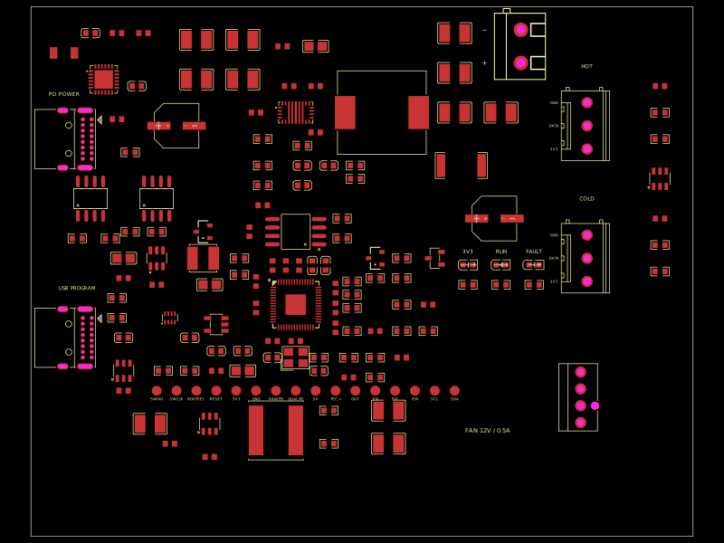 More from this authorabse/dual-usb-peltier-assemblyA USB‑C PD Peltier controller PCB combining RP2040 control, adjustable buck‑boost TEC power, temperature sensing, fan regulation, USB programming, protection, status LEDs, and external accessory hardware.
 Similar packagemohan-bee/esp32-c3This hardware design integrates an ESP32-C3 microcontroller, a USB-C connector, a power management IC (AP2112-3.3V regulator), a USB-to-Serial converter (CH340C), several resistors, capacitors, and user-accessible headers to facilitate USB communication, power regulation, and general I/O interfacing.
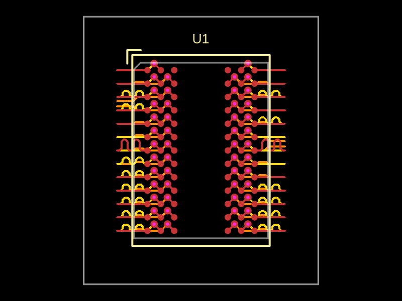 Discover something new0hmX/mt41k512m8da-107-it-p-fanoutThis code defines the physical footprint, routing, and layout configuration for a DDR3 memory module using surface-mount pads, vias, and copper traces on a printed circuit board (PCB).