abse/gameboy-advance
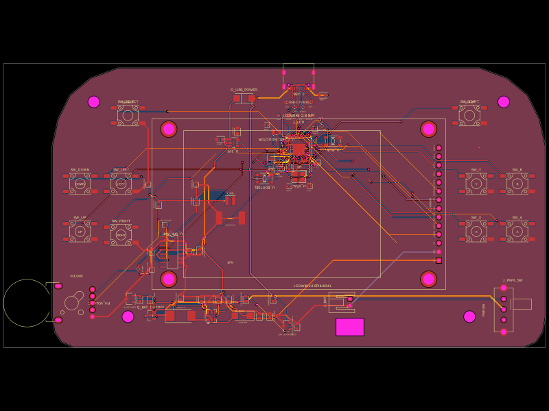
This code defines a collection of hardware components, including microcontrollers, sensors, display modules, power management ICs, and passive/passive components, each modeled as 3D symbols with specific footprints, pin configurations, and associated models for PCB and schematic design.
- Version
- 0.0.10
- License
- unset
- Stars
- 0
index.circuit.tsx
PCB
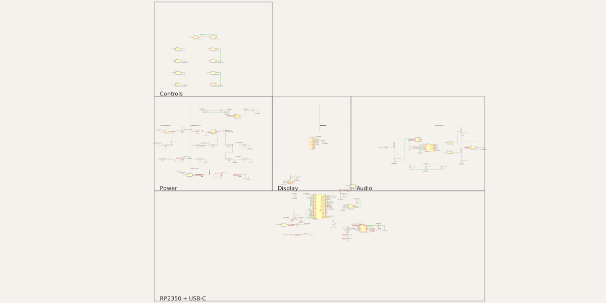
Schematic
import { PowerBoost_MT3608 } from "./subcircuits/PowerBoost_MT3608/PowerBoost_MT3608.circuit"
import { AudioAmplifier3W_PAM8403 } from "./subcircuits/AudioAmplifier3W_PAM8403/AudioAmplifier3W_PAM8403.circuit"
import { LCDWiki_2_8_SPI_ILI9341_MSP2807 } from "./imports/LCDWiki_2_8_SPI_ILI9341_MSP2807"
import { KH_6X6X15H_SMT_FS_D } from "./imports/KH_6X6X15H_SMT_FS_D"
import { SK_12E12_G5 } from "./imports/SK_12E12_G5"
import { Microcontroller_RP2350 } from "./Microcontroller_RP2350.circuit"
import { AP2112K_3_3TRG1 } from "./imports/AP2112K_3_3TRG1"
import { SS34 } from "./imports/SS34"

const denseTraceProps = { thickness: "0.1mm" } as const
const batteryTraceProps = { thickness: "0.3mm" } as const
const powerTraceProps = { thickness: "0.4mm" } as const
const gndLabel = { displayName: "GND", schDisplayLabel: "GND" } as const
const v3v3Label = { displayName: "V3V3", schDisplayLabel: "V3V3" } as const
const vsysLabel = { displayName: "VSYS", schDisplayLabel: "VSYS" } as const
const vbusLabel = { displayName: "VBUS", schDisplayLabel: "VBUS" } as const

const schSections = {
  power: "power",
  controls: "controls",
  display: "display",
} as const

export default ({
  mcuSubcircuit = false,
  layers = 4,
  copperIslands = true,
}: { mcuSubcircuit?: boolean; layers?: 2 | 4; copperIslands?: boolean } = {}) => (
  <board
    title="Game Boy Advance RP2350 handheld circuit"
    autorouter="beta-pipeline9"
    width="144.5mm"
    height="82mm"
    layers={layers}
    minViaHoleDiameter="0.3mm"
    minViaPadDiameter="0.45mm"
    outline={[
      { x: -66, y: -41 },
      { x: 66, y: -41 },
      { x: 69.5, y: -39.5 },
      { x: 71.5, y: -36.5 },
      { x: 72.25, y: -32 },
      { x: 72.25, y: 18 },
      { x: 70.5, y: 26 },
      { x: 67, y: 33 },
      { x: 61, y: 38 },
      { x: 53, y: 41 },
      { x: -53, y: 41 },
      { x: -61, y: 38 },
      { x: -67, y: 33 },
      { x: -70.5, y: 26 },
      { x: -72.25, y: 18 },
      { x: -72.25, y: -32 },
      { x: -71.5, y: -36.5 },
      { x: -69.5, y: -39.5 },
    ]}
  >
    <schematicrect schX={0} schY={-10} width={84} height={28} strokeWidth={0.08} color="#777777" />
    <schematictext text="RP2350 + USB-C" schX={-40.6} schY={-22.4} fontSize={1.4} anchor="top_left" color="#333333" />
    <schematicrect schX={-27} schY={16} width={30} height={24} strokeWidth={0.08} color="#777777" />
    <schematictext text="Power" schX={-40.6} schY={5.6} fontSize={1.4} anchor="top_left" color="#333333" />
    <schematicrect schX={-2} schY={16} width={20} height={24} strokeWidth={0.08} color="#777777" />
    <schematictext text="Display" schX={-10.6} schY={5.6} fontSize={1.4} anchor="top_left" color="#333333" />
    <schematicrect schX={25} schY={16} width={34} height={24} strokeWidth={0.08} color="#777777" />
    <schematictext text="Audio" schX={9.4} schY={5.6} fontSize={1.4} anchor="top_left" color="#333333" />
    <schematicrect schX={-27} schY={40} width={30} height={24} strokeWidth={0.08} color="#777777" />
    <schematictext text="Controls" schX={-40.6} schY={29.6} fontSize={1.4} anchor="top_left" color="#333333" />

    <net name="GND" isGroundNet />
    <net name="V3V3" isPowerNet />
    <net name="VSYS" isPowerNet />
    <net name="VBUS" isPowerNet />
    <net name="BAT_POS" isPowerNet />
    <net name="BAT_SWITCHED" isPowerNet />
    <net name="AUDIO_PWM" />

    <hole name="MH_TOP_LEFT" diameter="3.3mm" pcbX={-50} pcbY={-32} />
    <hole name="MH_TOP_RIGHT" diameter="3.3mm" pcbX={50} pcbY={-32} />
    <hole name="MH_BOTTOM_LEFT" diameter="3.3mm" pcbX={-60} pcbY={31} />
    <hole name="MH_BOTTOM_RIGHT" diameter="3.3mm" pcbX={60} pcbY={31} />

    <Microcontroller_RP2350
      name="MCU"
      subcircuit={mcuSubcircuit}
      pcbRotation={180}
      pcbX={0}
      pcbY={17}
    />

    <PowerBoost_MT3608
      name="POWER"
      pcbX={-32}
      pcbY={-53}
      schX={-29}
      schY={15}
    />
    <trace name="POWER_BAT_POS_INTERFACE" from="net.BAT_POS" to=".POWER > net.POWER_BAT_POS" {...batteryTraceProps} />
    <trace name="POWER_BAT_SWITCHED_INTERFACE" from="net.BAT_SWITCHED" to=".POWER > net.POWER_BAT_SWITCHED" {...batteryTraceProps} />
    <trace name="POWER_VBUS_INTERFACE" from="net.VBUS" to=".POWER > net.POWER_VBUS" {...powerTraceProps} />
    <trace name="POWER_VSYS_INTERFACE" from="net.VSYS" to=".POWER > net.POWER_VSYS" {...powerTraceProps} />
    <trace name="POWER_GND_INTERFACE" from="net.GND" to=".POWER > net.POWER_GND" {...gndLabel} />

    <trace
      name="USB_VBUS_TO_POWER"
      from=".MCU .J_USB > .A4B9"
      to="net.VBUS"
      {...powerTraceProps}
      {...vbusLabel}
    />
    <trace
      name="MCU_GND"
      from=".MCU .U1 > .GND"
      to="net.GND"
      {...gndLabel}
    />
    <trace
      name="MCU_V3V3"
      from=".MCU .U1 > .VREG_VIN"
      to="net.V3V3"
      {...powerTraceProps}
      {...v3v3Label}
    />

    {/* USB feeds VSYS through a diode; the common power circuit disables
        its battery boost when VBUS is present. The diode blocks backfeed. */}
    <SS34 name="D_USB_POWER" pcbX={-16} pcbY={32} schX={-29} schY={24} />
    <trace name="USB_POWER_IN" from="net.VBUS" to=".D_USB_POWER > .anode" {...powerTraceProps} />
    <trace name="USB_POWER_OUT" from=".D_USB_POWER > .cathode" to="net.VSYS" {...powerTraceProps} />

    {/* The MCU's internal regulator only generates 1.1 V; its I/O and
        regulator input require this external 3.3 V supply. */}
    <AP2112K_3_3TRG1
      name="U_3V3"
      pcbX={-19}
      pcbY={19}
      pcbRotation={180}
      schX={-21}
      schY={23}
      noConnect={["NC"]}
    />
    <capacitor name="C_3V3_IN" capacitance="1uF" maxDecouplingTraceLength="5.5mm" footprint="0603" supplierPartNumbers={{ jlcpcb: ["C15849"] }} pcbX={-23.2} pcbY={20} pcbRotation={180} schX={-25} schY={24.5} />
    <capacitor name="C_3V3_OUT" capacitance="1uF" maxDecouplingTraceLength="5.5mm" footprint="0603" supplierPartNumbers={{ jlcpcb: ["C15849"] }} pcbX={-17.9} pcbY={22.5} pcbRotation={90} schX={-17} schY={24.5} />
    <trace name="REG_3V3_IN" from="net.VSYS" to=".U_3V3 > .VIN" {...powerTraceProps} />
    <trace name="REG_3V3_ENABLE" from=".U_3V3 > .EN" to="net.VSYS" />
    <trace name="REG_3V3_GND" from=".U_3V3 > .GND" to="net.GND" />
    <trace name="REG_3V3_OUT" from=".U_3V3 > .VOUT" to="net.V3V3" {...powerTraceProps} />
    <trace name="REG_3V3_INPUT_CAP" from=".C_3V3_IN > .pin1" to=".U_3V3 > .VIN" maxLength="5.5mm" />
    <trace name="REG_3V3_INPUT_CAP_GND" from=".C_3V3_IN > .pin2" to="net.GND" />
    <trace name="REG_3V3_OUTPUT_CAP" from=".C_3V3_OUT > .pin1" to=".U_3V3 > .VOUT" maxLength="5.5mm" />
    <trace name="REG_3V3_OUTPUT_CAP_GND" from=".C_3V3_OUT > .pin2" to="net.GND" />

    <AudioAmplifier3W_PAM8403
      name="AUDIO"
      pcbX={-53}
      pcbY={-8}
      pcbRotation={0}
    schX={25}
      schY={12}
    />
    <trace name="AUDIO_PWM_INTERFACE" from="net.AUDIO_PWM" to=".AUDIO > net.AUDIO_PWM_INTERNAL" {...denseTraceProps} />
    <trace name="AUDIO_V3V3_INTERFACE" from="net.V3V3" to=".AUDIO > net.V3V3_INTERNAL" {...powerTraceProps} />
    <trace name="AUDIO_VSYS_INTERFACE" from="net.VSYS" to=".AUDIO > net.VSYS_INTERNAL" {...powerTraceProps} />
    <trace name="AUDIO_GND_INTERFACE" from="net.GND" to=".AUDIO > net.GND_INTERNAL" {...gndLabel} />
    <trace name="AUDIO_SIGNAL" from=".MCU .U1 > .GPIO22" to="net.AUDIO_PWM" />

    <LCDWiki_2_8_SPI_ILI9341_MSP2807
      name="J_LCD"
      schSectionName={schSections.display}
      layer="top"
      pcbX={0}
      pcbY={1}
      schX={-2}
      schY={16}
    />

    <cutout
      name="BAT_CABLE_SLOT"
      shape="rect"
      width="8mm"
      height="5mm"
      pcbX="15mm"
      pcbY="-35mm"
    />
    <SK_12E12_G5
      name="J_PWR_SW"
      schSectionName={schSections.power}
      pcbX={60}
      pcbY={-30}
      pcbRotation={0}
      schX={-33}
      schY={8}
      schHeight={0.6}
      noConnect={["pin3"]}
    />
    <trace name="BATTERY_TO_SWITCH" from="net.BAT_POS" to=".J_PWR_SW > .pin1" {...batteryTraceProps} />
    <trace name="SWITCH_TO_BOOST" from=".J_PWR_SW > .pin2" to="net.BAT_SWITCHED" {...batteryTraceProps} />

    <KH_6X6X15H_SMT_FS_D name="SW_UP" schSectionName={schSections.controls} pcbX={-64} pcbY={-7} schX={-36} schY={31} />
    <KH_6X6X15H_SMT_FS_D name="SW_DOWN" schSectionName={schSections.controls} pcbX={-64} pcbY={7} schX={-36} schY={34} />
    <KH_6X6X15H_SMT_FS_D name="SW_LEFT" schSectionName={schSections.controls} pcbX={-52} pcbY={7} schX={-36} schY={37} />
    <KH_6X6X15H_SMT_FS_D name="SW_RIGHT" schSectionName={schSections.controls} pcbX={-52} pcbY={-8} schX={-36} schY={40} />
    <KH_6X6X15H_SMT_FS_D name="SW_A" schSectionName={schSections.controls} pcbX={64} pcbY={-7} schX={-27} schY={31} />
    <KH_6X6X15H_SMT_FS_D name="SW_B" schSectionName={schSections.controls} pcbX={64} pcbY={7} schX={-27} schY={34} />
    <KH_6X6X15H_SMT_FS_D name="SW_X" schSectionName={schSections.controls} pcbX={52} pcbY={-7} schX={-27} schY={37} />
    <KH_6X6X15H_SMT_FS_D name="SW_Y" schSectionName={schSections.controls} pcbX={52} pcbY={7} schX={-27} schY={40} />
    <KH_6X6X15H_SMT_FS_D name="SW_SELECT" schSectionName={schSections.controls} pcbX={-50} pcbY={27} schX={-31.5} schY={43} />
    <KH_6X6X15H_SMT_FS_D name="SW_START" schSectionName={schSections.controls} pcbX={50} pcbY={27} schX={-27} schY={43} />

    <trace name="UP" from=".SW_UP > .pin1" to=".MCU .U1 > .GPIO2" />
    <trace name="UP_G" from=".SW_UP > .pin4" to="net.GND" {...gndLabel} />
    <trace name="DN" from=".SW_DOWN > .pin1" to=".MCU .U1 > .GPIO3" />
    <trace name="DN_G" from=".SW_DOWN > .pin4" to="net.GND" {...gndLabel} />
    <trace name="LFT" from=".SW_LEFT > .pin1" to=".MCU .U1 > .GPIO4" />
    <trace name="LFT_G" from=".SW_LEFT > .pin4" to="net.GND" {...gndLabel} />
    <trace name="RGT" from=".SW_RIGHT > .pin1" to=".MCU .U1 > .GPIO5" />
    <trace name="RGT_G" from=".SW_RIGHT > .pin4" to="net.GND" {...gndLabel} />
    <trace name="A" from=".SW_A > .pin1" to=".MCU .U1 > .GPIO6" />
    <trace name="A_G" from=".SW_A > .pin4" to="net.GND" {...gndLabel} />
    <trace name="B" from=".SW_B > .pin1" to=".MCU .U1 > .GPIO7" />
    <trace name="B_G" from=".SW_B > .pin4" to="net.GND" {...gndLabel} />
    <trace name="X" from=".SW_X > .pin1" to=".MCU .U1 > .GPIO8" />
    <trace name="X_G" from=".SW_X > .pin4" to="net.GND" {...gndLabel} />
    <trace name="Y" from=".SW_Y > .pin1" to=".MCU .U1 > .GPIO9" />
    <trace name="Y_G" from=".SW_Y > .pin4" to="net.GND" {...gndLabel} />
    <trace name="SEL" from=".SW_SELECT > .pin1" to=".MCU .U1 > .GPIO10" />
    <trace name="SEL_G" from=".SW_SELECT > .pin4" to="net.GND" {...gndLabel} />
    <trace name="STA" from=".SW_START > .pin1" to=".MCU .U1 > .GPIO11" />
    <trace name="STA_G" from=".SW_START > .pin4" to="net.GND" {...gndLabel} />

    <trace name="LCD_VCC" from=".J_LCD .J_HEADER > .VCC" to="net.VSYS" {...powerTraceProps} {...vsysLabel} />
    <trace name="LCD_GND" from=".J_LCD .J_HEADER > .GND" to="net.GND" {...gndLabel} />
    <trace name="LCD_CS" from=".J_LCD .J_HEADER > .CS" to=".MCU .U1 > .GPIO17" />
    <trace name="LCD_RST" from=".J_LCD .J_HEADER > .RESET" to=".MCU .U1 > .GPIO21" />
    <trace name="LCD_DC" from=".J_LCD .J_HEADER > .DC_RS" to=".MCU .U1 > .GPIO20" />
    <trace name="LCD_MOSI" from=".J_LCD .J_HEADER > .SDI_MOSI" to=".MCU .U1 > .GPIO19" />
    <trace name="LCD_SCK" from=".J_LCD .J_HEADER > .SCK" to=".MCU .U1 > .GPIO18" />
    <trace name="LCD_LED" from=".J_LCD .J_HEADER > .LED" to="net.V3V3" {...v3v3Label} />
    <trace name="LCD_MISO" from=".J_LCD .J_HEADER > .SDO_MISO" to=".MCU .U1 > .GPIO16" />

    <trace name="SW_G" from=".J_PWR_SW > .pin4" to="net.GND" {...gndLabel} />
    <trace name="SW_G2" from=".J_PWR_SW > .pin5" to="net.GND" {...gndLabel} />

    <copperpour
      name="GND_POUR_TOP"
      connectsTo="net.GND"
      layer="top"
      clearance="0.18mm"
      boardEdgeMargin="0.25mm"
    />
    <copperpour
      name="GND_POUR_BOTTOM"
      connectsTo="net.GND"
      layer="bottom"
      clearance="0.18mm"
      boardEdgeMargin="0.25mm"
    />

    {/* Like the RP2350 reference, keep each supply region local to its
        regulator and capacitor. Coordinates are board coordinates. These
        pours supplement real net connections; no route is disabled. */}
    {copperIslands && (
      <copperpour
        name="V3V3_REGULATOR_ISLAND"
        connectsTo="net.V3V3"
        layer="top"
        clearance="0.18mm"
        boardEdgeMargin={0}
        outline={[
          { x: -18.5, y: 19.2 },
          { x: -17.3, y: 19.2 },
          { x: -17.3, y: 22.2 },
          { x: -18.5, y: 22.2 },
        ]}
      />
    )}
    {copperIslands && (
      <copperpour
        name="V1V1_REGULATOR_ISLAND"
        connectsTo=".MCU > net.V1V1"
        layer="top"
        clearance="0.18mm"
        boardEdgeMargin={0}
        outline={[
          { x: -8, y: 21.3 },
          { x: -6.9, y: 21.3 },
          { x: -6.9, y: 23.2 },
          { x: -8.5, y: 24.8 },
          { x: -9.35, y: 24.8 },
          { x: -9.35, y: 23.6 },
          { x: -8, y: 22.6 },
        ]}
      />
    )}

    <silkscreentext text="LCDWIKI 2.8 SPI" fontSize="1.2mm" pcbX={0} pcbY={27} />
    <silkscreentext text="BAT" fontSize="0.9mm" pcbX={15} pcbY={-29} />
    <silkscreentext text="USB-C / VBUS" fontSize="0.9mm" pcbX={0} pcbY={31} />
    <silkscreentext text="PWR SW" fontSize="0.9mm" pcbX={54} pcbY={-30} pcbRotation={90} />
    <silkscreentext text="UP" fontSize="0.9mm" pcbX={-64} pcbY={-7} />
    <silkscreentext text="DOWN" fontSize="0.9mm" pcbX={-64} pcbY={7} />
    <silkscreentext text="LEFT" fontSize="0.9mm" pcbX={-52} pcbY={7} />
    <silkscreentext text="RIGHT" fontSize="0.9mm" pcbX={-52} pcbY={-8} />
    <silkscreentext text="A" fontSize="0.9mm" pcbX={64} pcbY={-7} />
    <silkscreentext text="B" fontSize="0.9mm" pcbX={64} pcbY={7} />
    <silkscreentext text="X" fontSize="0.9mm" pcbX={52} pcbY={-7} />
    <silkscreentext text="Y" fontSize="0.9mm" pcbX={52} pcbY={7} />
    <silkscreentext text="SELECT" fontSize="0.9mm" pcbX={-50} pcbY={31} />
    <silkscreentext text="START" fontSize="0.9mm" pcbX={50} pcbY={31} />
    <silkscreentext text="VOLUME" fontSize="0.9mm" pcbX={-65} pcbY={-20} />
    <silkscreentext text="SPK" fontSize="0.9mm" pcbX={-20} pcbY={-16} />
  </board>
)
Related Packages
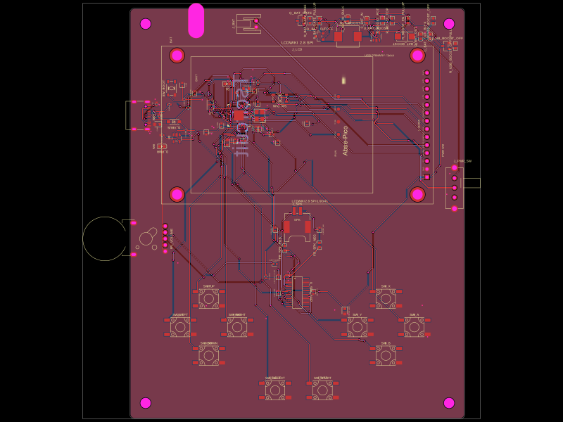 More from this authorabse/gameboyThis code defines the hardware mapping and schematic connections for a Raspberry Pi Pico-based development board featuring RP2040 microcontroller, USB-C connector, various power regulation components, decoupling capacitors, resistors, LEDs, headers, and supporting passive components for signal integrity and debugging.
 Similar packageaura/diy-power-delivery-triggerThis hardware design implements a USB Type-C port with supporting power management and signal conditioning components, including a USB-C connector, a FUSB302 USB-C port controller, ESD protection diodes, a buck converter for 3.3V power regulation, an STM32 microcontroller for control and processing, an RGB LED indicator, push button, terminal block connections, and associated filtering and support components.
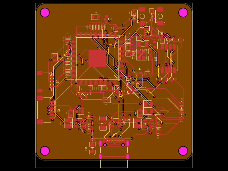 Discover something newtechmannih/trellis-coreThis code defines a detailed electronic hardware schematic and PCB layout for a Linux System-on-Module, incorporating components such as oscillators, power regulators, USB-C connectors, connectors, LEDs, resistors, capacitors, inductors, and integrated circuits, with precise physical footprint and 3D models.