abse/gameboy-advance
A tscircuit package created by abse.
- Version
- 0.0.45
- License
- unset
- Stars
- 0
firmware/game-console/sd-fatfs/sd_driver/SDIO/rp2040_sdio.pio
; RP2040 PIO program for implementing SD card access in SDIO mode
; Run "pioasm rp2040_sdio.pio rp2040_sdio.pio.h" to regenerate the C header from this.

; The RP2040 official work-in-progress code at
; https://github.com/raspberrypi/pico-extras/tree/master/src/rp2_common/pico_sd_card
; may be useful reference, but this is independent implementation.
;
; For official SDIO specifications, refer to:
; https://www.sdcard.org/downloads/pls/
; "SDIO Physical Layer Simplified Specification Version 8.00"

; Clock settings
; For 3.3V communication the available speeds are:
; - Default speed: max. 25 MHz clock
; - High speed:    max. 50 MHz clock
;
; From the default RP2040 clock speed of 125 MHz, the closest dividers
; are 3 for 41.7 MHz and 5 for 25 MHz. The CPU can apply further divider
; through state machine registers for the initial handshake.
;
; Because data is written on the falling edge and read on the rising
; edge, it is preferrable to have a long 0 state and short 1 state.
;.define CLKDIV 3
;.define CLKDIV 5
;.define D0 ((CLKDIV + 1) / 2 - 1)
;.define D1 (CLKDIV/2 - 1)

.define D0 1
.define D1 1
.define PUBLIC CLKDIV D0 + 1 + D1 + 1

; .define PUBLIC SDIO_CLK_GPIO 17

; This is relative to D0 GPIO number.
; The pin is selected by adding Index to the
;   PINCTRL_IN_BASE configuration, modulo 32.
; This is used as a WAIT index, and must be between 4 and 31.
; (Offsets 0-3 are D0, D1, D2, and D3.)
.define PUBLIC SDIO_CLK_PIN_D0_OFFSET 30    ; (-2 in mod32 arithmetic)

; State machine 0 is used to:
; - generate continuous clock on SDIO_CLK
; - send CMD packets
; - receive response packets
;
; Pin mapping for this state machine:
; - Sideset    : CLK
; - IN/OUT/SET : CMD
; - JMP_PIN    : CMD
;
; The commands to send are put on TX fifo and must have two words:
; Word 0 bits 31-24: Number of bits in command minus one (usually 47)
; Word 0 bits 23-00: First 24 bits of the command packet, shifted out MSB first
; Word 1 bits 31-08: Last 24 bits of the command packet, shifted out MSB first
; Word 1 bits 07-00: Number of bits in response minus one (usually 47), or 0 if no response
;
; The response is put on RX fifo, starting with the MSB.
; Partial last word will be padded with zero bits at the top.
;
; The state machine EXECCTRL should be set so that STATUS indicates TX FIFO < 2
; and that AUTOPULL and AUTOPUSH are enabled.

.program sdio_cmd_clk
    .side_set 1

    mov OSR, NULL       side 1 [D1]    ; Make sure OSR is full of zeros to prevent autopull

wait_cmd:
    mov Y, !STATUS      side 0 [D0]    ; Check if TX FIFO has data
    jmp !Y wait_cmd     side 1 [D1]

load_cmd:
    out NULL, 32        side 0 [D0]    ; Load first word (trigger autopull)
    out X, 8            side 1 [D1]    ; Number of bits to send
    set pins, 1         side 0 [D0]    ; Initial state of CMD is high
    set pindirs, 1      side 1 [D1]    ; Set SDIO_CMD as output

send_cmd:
    out pins, 1         side 0 [D0]    ; Write output on falling edge of CLK
    jmp X-- send_cmd    side 1 [D1]

prep_resp:
    set pindirs, 0      side 0 [D0]    ; Set SDIO_CMD as input
    out X, 8            side 1 [D1]    ; Get number of bits in response
    nop                 side 0 [D0]    ; For clock alignment
    jmp !X resp_done    side 1 [D1]    ; Check if we expect a response

wait_resp:
    nop                  side 0 [D0]
    jmp PIN wait_resp    side 1 [D1]    ; Loop until SDIO_CMD = 0

    ; Note: input bits are read at the same time as we write CLK=0.
    ; Because the host controls the clock, the read happens before
    ; the card sees the falling clock edge. This gives maximum time
    ; for the data bit to settle.
read_resp:
    in PINS, 1          side 0 [D0]    ; Read input data bit
    jmp X-- read_resp   side 1 [D1]    ; Loop to receive all data bits

resp_done:
    push                side 0 [D0]    ; Push the remaining part of response

; State machine 1 is used to send and receive data blocks.
; Pin mapping for this state machine:
; - IN / OUT: SDIO_D0-D3
; - GPIO defined at beginning of this file: SDIO_CLK

; Data reception program
; This program will wait for initial start of block token and then
; receive a data block. The application must set number of nibbles
; to receive minus 1 to Y register before running this program.
.program sdio_data_rx

wait_start:
    mov X, Y                               ; Reinitialize number of nibbles to receive
    wait 0 pin 0                           ; Wait for zero state on D0
    wait 1 pin SDIO_CLK_PIN_D0_OFFSET  [CLKDIV-1]  ; Wait for rising edge and then whole clock cycle

rx_data:
    in PINS, 4                 [CLKDIV-2]  ; Read nibble
    jmp X--, rx_data

; Data transmission program
;
; Before running this program, pindirs should be set as output
; and register X should be initialized with the number of nibbles
; to send minus 1 (typically 8 + 1024 + 16 + 1 - 1 = 1048)
; and register Y with the number of response bits minus 1 (typically 31).
;
; Words written to TX FIFO must be:
; - Word 0: start token 0xFFFFFFF0
; - Word 1-128: transmitted data (512 bytes)
; - Word 129-130: CRC checksum
; - Word 131: end token 0xFFFFFFFF
;
; After the card reports idle status, RX FIFO will get a word that
; contains the D0 line response from card.

.program sdio_data_tx
    wait 0 pin SDIO_CLK_PIN_D0_OFFSET
    wait 1 pin SDIO_CLK_PIN_D0_OFFSET  [CLKDIV + D1 - 1]; Synchronize so that write occurs on falling edge

tx_loop:
    out PINS, 4                [D0]    ; Write nibble and wait for whole clock cycle
    jmp X-- tx_loop            [D1]

    set pindirs, 0x00          [D0]    ; Set data bus as input

.wrap_target
response_loop:
    in PINS, 1                 [D1]    ; Read D0 on rising edge
    jmp Y--, response_loop     [D0]

wait_idle:
    wait 1 pin 0               [D1]    ; Wait for card to indicate idle condition
    push                       [D0]    ; Push the response token
.wrap
Related Packages
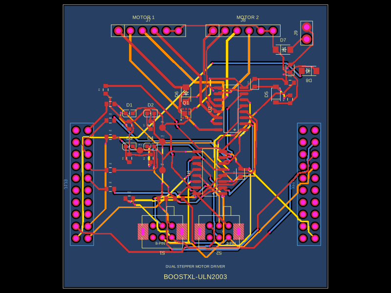 More from this authorabse/boostxl-uln2003This code defines a React component that models a through-hole or surface-mount LED with specified pin labels, footprint, silkscreen, and 3D CAD model for PCB layout.
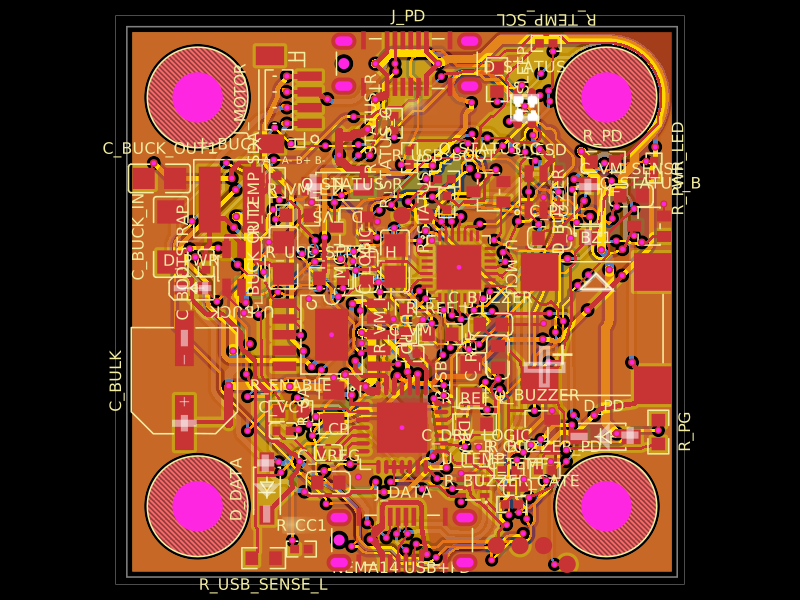 Discover something newAnasSarkiz/NEMA14_CH32X035G8U6A NEMA stepper motor is shown with proposed M3 screws/spacers, four wired motor leads and splices, and a JST SHR-04V-S connector.