abse/boostxl-tmp107
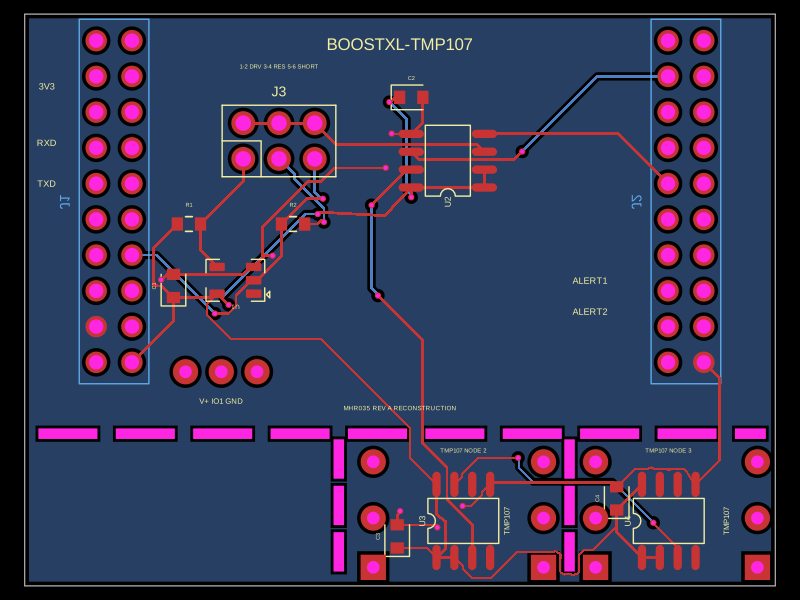
This code defines a 6-pin electronic component with a specified footprint, 3D models, and pin labels, suitable for PCB design and visualization.
- Version
- 1.0.7
- License
- unset
- Stars
- 0
index.circuit.tsx
PCB
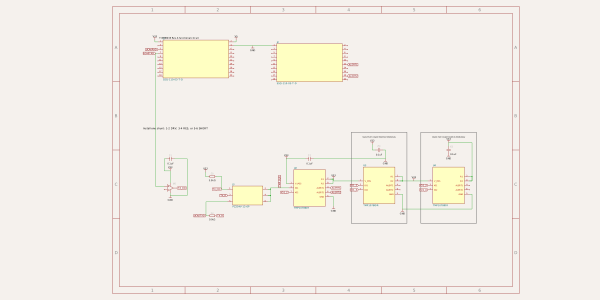
Schematic
import { PZ254V_12_6P } from "./imports/PZ254V_12_6P/PZ254V_12_6P"
import { SN74LVC1G07DBVR } from "./imports/SN74LVC1G07DBVR/SN74LVC1G07DBVR"
import { SSQ_110_03_T_D } from "./imports/SSQ_110_03_T_D/SSQ_110_03_T_D"
import { TMP107BIDR } from "./imports/TMP107BIDR/TMP107BIDR"

const N = {
  V5: "net.V5",
  V33: "net.V33",
  GND: "net.GND",
  RXD: "net.UCA0RXD",
  TXD: "net.UCA0TXD",
  TX_OD: "net.TX_OD",
  TX_R: "net.TX_R",
  BUS: "net.TMP_BUS",
  ALERT1: "net.ALERT1",
  ALERT2: "net.ALERT2",
  IO12: "net.IO1_2",
  IO13: "net.IO1_3",
  IO14: "net.IO1_4",
} as const

const HEADER_SCH_PIN_STYLE = {
  pin1: { marginTop: "0.05mm", marginBottom: "0.05mm" },
  pin2: { marginTop: "0.05mm", marginBottom: "0.05mm" },
  pin3: { marginTop: "0.05mm", marginBottom: "0.05mm" },
  pin4: { marginTop: "0.05mm", marginBottom: "0.05mm" },
  pin5: { marginTop: "0.05mm", marginBottom: "0.05mm" },
  pin6: { marginTop: "0.05mm", marginBottom: "0.05mm" },
  pin7: { marginTop: "0.05mm", marginBottom: "0.05mm" },
  pin8: { marginTop: "0.05mm", marginBottom: "0.05mm" },
  pin9: { marginTop: "0.05mm", marginBottom: "0.05mm" },
  pin10: { marginTop: "0.05mm", marginBottom: "0.05mm" },
  pin11: { marginTop: "0.05mm", marginBottom: "0.05mm" },
  pin12: { marginTop: "0.05mm", marginBottom: "0.05mm" },
  pin13: { marginTop: "0.05mm", marginBottom: "0.05mm" },
  pin14: { marginTop: "0.05mm", marginBottom: "0.05mm" },
  pin15: { marginTop: "0.05mm", marginBottom: "0.05mm" },
  pin16: { marginTop: "0.05mm", marginBottom: "0.05mm" },
  pin17: { marginTop: "0.05mm", marginBottom: "0.05mm" },
  pin18: { marginTop: "0.05mm", marginBottom: "0.05mm" },
  pin19: { marginTop: "0.05mm", marginBottom: "0.05mm" },
  pin20: { marginTop: "0.05mm", marginBottom: "0.05mm" },
}

const TMP107_SCH_PIN_STYLE = {
  pin1: { marginTop: "0.075mm", marginBottom: "0.075mm" },
  pin2: { marginTop: "0.075mm", marginBottom: "0.075mm" },
  pin3: { marginTop: "0.075mm", marginBottom: "0.075mm" },
  pin4: { marginTop: "0.075mm", marginBottom: "0.075mm" },
  pin5: { marginTop: "0.075mm", marginBottom: "0.075mm" },
  pin6: { marginTop: "0.075mm", marginBottom: "0.075mm" },
  pin7: { marginTop: "0.075mm", marginBottom: "0.075mm" },
  pin8: { marginTop: "0.075mm", marginBottom: "0.075mm" },
}

const SHUNT_HEADER_SCH_PIN_STYLE = {
  pin1: { marginTop: "0.15mm", marginBottom: "0.15mm" },
  pin2: { marginTop: "0.15mm", marginBottom: "0.15mm" },
  pin3: { marginTop: "0.15mm", marginBottom: "0.15mm" },
  pin4: { marginTop: "0.15mm", marginBottom: "0.15mm" },
  pin5: { marginTop: "0.15mm", marginBottom: "0.15mm" },
  pin6: { marginTop: "0.15mm", marginBottom: "0.15mm" },
}

export default function Circuit() {
  return (
    <board
      name="BOOSTXL_TMP107"
      width="53.34mm"
      height="40.64mm"
      outline={[
        { x: -26.67, y: -20.32 },
        { x: 26.67, y: -20.32 },
        { x: 26.67, y: 20.32 },
        { x: -26.67, y: 20.32 },
      ]}
      solderMaskColor="red"
      silkscreenColor="white"
      defaultTraceWidth="0.2mm"
      minViaHoleDiameter="0.3mm"
      minViaPadDiameter="0.45mm"
      autorouter={{
        preset: "auto_local",
        local: true,
        traceClearance: "0.15mm",
      }}
      autorouterEffortLevel="2x"
    >
      <schematicsheet
        name="BOOSTXL-TMP107 Complete Schematic"
        displayName="BOOSTXL-TMP107 Complete Schematic"
        sheetIndex={1}
      />

      <group
        name="COMPLETE_SCHEMATIC"
        schSheetName="BOOSTXL-TMP107 Complete Schematic"
        schX={0}
        schY={0}
        pcbX={0}
        pcbY={0}
        schMaxTraceDistance="1.2mm"
        schTraceAutoLabelEnabled
      >
        <schematicsection
          name="TI_MHR035_FUNCTIONAL_CIRCUIT"
          displayName="TI MHR035 Rev A functional circuit"
          sectionTitleFontSize="0.18mm"
        />
        <SSQ_110_03_T_D
          name="J1"
          layer="bottom"
          schSectionName="TI_MHR035_FUNCTIONAL_CIRCUIT"
          schX={-9.5}
          schY={7.2}
          schWidth="5.2mm"
          schHeight="3mm"
          schPinStyle={HEADER_SCH_PIN_STYLE}
          schPinArrangement={{
            leftSide: [1, 3, 5, 7, 9, 11, 13, 15, 17, 19],
            rightSide: [2, 4, 6, 8, 10, 12, 14, 16, 18, 20],
          }}
          pcbX={-20.32}
          pcbY={7.0}
          pcbRotation={90}
          noConnect={["pin3", "pin6", "pin8", "pin9", "pin10", "pin11", "pin12", "pin13", "pin14", "pin15", "pin16", "pin17", "pin18", "pin19", "pin20"]}
          connections={{
            pin1: N.V33,
            pin2: N.V5,
            pin4: N.GND,
            pin5: N.RXD,
            pin7: N.TXD,
          }}
        />
        <SSQ_110_03_T_D
          name="J2"
          layer="bottom"
          schSectionName="TI_MHR035_FUNCTIONAL_CIRCUIT"
          schX={-0.5}
          schY={6.9}
          schWidth="5.2mm"
          schHeight="3mm"
          schPinStyle={HEADER_SCH_PIN_STYLE}
          schPinArrangement={{
            leftSide: [1, 3, 5, 7, 9, 11, 13, 15, 17, 19],
            rightSide: [2, 4, 6, 8, 10, 12, 14, 16, 18, 20],
          }}
          pcbX={20.32}
          pcbY={7.0}
          pcbRotation={90}
          noConnect={["pin2", "pin3", "pin4", "pin5", "pin6", "pin7", "pin8", "pin9", "pin10", "pin11", "pin13", "pin14", "pin15", "pin16", "pin17", "pin19", "pin20"]}
          connections={{
            pin1: N.GND,
            pin12: N.ALERT1,
            pin18: N.ALERT2,
          }}
        />
        <schematictext
          text="Install one shunt: 1-2 DRV, 3-4 RES, or 5-6 SHORT"
          schX={-13.7}
          schY={1.7}
          fontSize={0.2}
          anchor="center_left"
        />
        <SN74LVC1G07DBVR
          name="U1"
          schSectionName="TI_MHR035_FUNCTIONAL_CIRCUIT"
          noSchematicRepresentation
          pcbX={-11.7}
          pcbY={1.4}
          noConnect={["NC"]}
          connections={{
            A: N.TXD,
            GND: N.GND,
            Y: N.TX_OD,
            VCC: N.V33,
          }}
        />
        {/* Keep TI's exact JLCPCB buffer package on the PCB, but project it as
            the native powered-triangle symbol used by the reference sheet. */}
        <schematicsymbol
          name="U1_BUFFER"
          displayName="U1"
          chipRef=".U1"
          symbolName="opamp_with_power"
          schSectionName="TI_MHR035_FUNCTIONAL_CIRCUIT"
          schX={-11.5}
          schY={-3}
          connections={{
            inp1: ".U1 > .A",
            inp2: ".U1 > .NC",
            out: ".U1 > .Y",
            "V+": ".U1 > .VCC",
            "V-": ".U1 > .GND",
          }}
        />
        <capacitor
          name="C1"
          schSectionName="TI_MHR035_FUNCTIONAL_CIRCUIT"
          schX={-11.5}
          schY={-0.7}
          schRotation="0deg"
          manufacturerPartNumber="GRM188R71E104KA01D"
          supplierPartNumbers={{ jlcpcb: ["C77050"] }}
          capacitance="0.1uF"
          footprint="0603"
          pcbX={-16.1}
          pcbY={1.0}
          pcbRotation={90}
          connections={{ pin1: N.V33, pin2: N.GND }}
        />
        <resistor
          name="R1"
          schSectionName="TI_MHR035_FUNCTIONAL_CIRCUIT"
          schX={-8.2}
          schY={-2.1}
          schRotation="0deg"
          manufacturerPartNumber="0603WAF3301T5E"
          supplierPartNumbers={{ jlcpcb: ["C22978"] }}
          resistance="3.3kohm"
          footprint="0603"
          pcbX={-15.0}
          pcbY={5.4}
          connections={{ pin1: N.V33, pin2: N.TX_OD }}
        />
        <resistor
          name="R2"
          schSectionName="TI_MHR035_FUNCTIONAL_CIRCUIT"
          schX={-8.2}
          schY={-5.2}
          manufacturerPartNumber="CQ03WAF1002T5E"
          supplierPartNumbers={{ jlcpcb: ["C516551"] }}
          resistance="10kohm"
          footprint="0603"
          pcbX={-7.6}
          pcbY={5.4}
          connections={{ pin1: N.TXD, pin2: N.TX_R }}
        />
        <PZ254V_12_6P
          name="J3"
          schSectionName="TI_MHR035_FUNCTIONAL_CIRCUIT"
          schX={-5.4}
          schY={-3.6}
          schWidth="2.4mm"
          schHeight="1.5mm"
          schPinStyle={SHUNT_HEADER_SCH_PIN_STYLE}
          schPinArrangement={{ leftSide: [1, 3, 5], rightSide: [2, 4, 6] }}
          pcbX={-8.6}
          pcbY={11.3}
          connections={{
            pin1: N.TX_OD,
            pin2: N.BUS,
            pin3: N.TX_R,
            pin4: N.BUS,
            pin5: N.TXD,
            pin6: N.BUS,
          }}
        />
        <TMP107BIDR
          name="U2"
          schSectionName="TI_MHR035_FUNCTIONAL_CIRCUIT"
          schX={-0.5}
          schY={-3}
          schWidth="2.5mm"
          schHeight="2.9mm"
          schPinStyle={TMP107_SCH_PIN_STYLE}
          schPinArrangement={{
            leftSide: [1, 3, 7],
            rightSide: [2, 8, 4, 6, 5],
          }}
          pcbX={3.4}
          pcbY={9.9}
          pcbRotation={90}
          connections={{
            V_POS: N.V33,
            R1: N.V33,
            IO1: N.BUS,
            ALERT1: N.ALERT1,
            GND: N.GND,
            ALERT2: N.ALERT2,
            IO2: N.IO12,
            R2: N.V33,
          }}
        />
        <capacitor
          name="C2"
          schSectionName="TI_MHR035_FUNCTIONAL_CIRCUIT"
          schX={-0.5}
          schY={-0.7}
          schRotation="0deg"
          manufacturerPartNumber="GRM188R71E104KA01D"
          supplierPartNumbers={{ jlcpcb: ["C77050"] }}
          capacitance="0.1uF"
          footprint="0603"
          pcbX={0.8}
          pcbY={14.4}
          connections={{ pin1: N.V33, pin2: N.GND }}
        />
        <TMP107BIDR
          name="U3"
          schSectionName="TI_MHR035_FUNCTIONAL_CIRCUIT"
          schX={5}
          schY={-2.8}
          schWidth="2.5mm"
          schHeight="2.9mm"
          schPinStyle={TMP107_SCH_PIN_STYLE}
          schPinArrangement={{
            leftSide: [1, 3, 7],
            rightSide: [2, 8, 4, 6, 5],
          }}
          pcbX={4.5}
          pcbY={-15.7}
          pcbRotation={0}
          noConnect={["ALERT1", "ALERT2"]}
          connections={{
            V_POS: N.V33,
            R1: N.V33,
            IO1: N.IO12,
            GND: N.GND,
            IO2: N.IO13,
            R2: N.V33,
          }}
        />
        <capacitor
          name="C3"
          schSectionName="TI_MHR035_FUNCTIONAL_CIRCUIT"
          schX={5}
          schY={0}
          schRotation="0deg"
          manufacturerPartNumber="GRM188R71E104KA01D"
          supplierPartNumbers={{ jlcpcb: ["C77050"] }}
          capacitance="0.1uF"
          footprint="0603"
          pcbX={-0.2}
          pcbY={-16.8}
          pcbRotation={90}
          connections={{ pin1: N.V33, pin2: N.GND }}
        />
        <TMP107BIDR
          name="U4"
          schSectionName="TI_MHR035_FUNCTIONAL_CIRCUIT"
          schX={10.5}
          schY={-2.8}
          schWidth="2.5mm"
          schHeight="2.9mm"
          schPinStyle={TMP107_SCH_PIN_STYLE}
          schPinArrangement={{
            leftSide: [1, 3, 7],
            rightSide: [2, 8, 4, 6, 5],
          }}
          pcbX={19.1}
          pcbY={-15.7}
          pcbRotation={0}
          noConnect={["ALERT1", "ALERT2"]}
          connections={{
            V_POS: N.V33,
            R1: N.V33,
            IO1: N.IO13,
            GND: N.GND,
            IO2: N.IO14,
            R2: N.V33,
          }}
        />
        <capacitor
          name="C4"
          schSectionName="TI_MHR035_FUNCTIONAL_CIRCUIT"
          schX={10.5}
          schY={0}
          schRotation="270deg"
          manufacturerPartNumber="GRM188R71E104KA01D"
          supplierPartNumbers={{ jlcpcb: ["C77050"] }}
          capacitance="0.1uF"
          footprint="0603"
          pcbX={15.4}
          pcbY={-14.1}
          pcbRotation={90}
          connections={{ pin1: N.V33, pin2: N.GND }}
        />
        <schematicrect
          schX={5}
          schY={-2.2}
          width="4.4mm"
          height="7.2mm"
          strokeWidth="0.03mm"
          color="#555555"
        />
        <schematictext
          text="layout 3 pin coupon board as breakaway"
          schX={5}
          schY={1.05}
          fontSize={0.14}
          anchor="center"
        />
        <schematicrect
          schX={10.5}
          schY={-2.2}
          width="4.4mm"
          height="7.2mm"
          strokeWidth="0.03mm"
          color="#555555"
        />
        <schematictext
          text="layout 3 pin coupon board as breakaway"
          schX={10.5}
          schY={1.05}
          fontSize={0.14}
          anchor="center"
        />
      </group>

      {/* Main-board remote-chain pads. */}
      <platedhole name="MAIN_V33" shape="circle" outerDiameter="1.8mm" holeDiameter="0.9mm" pcbX={-15.24} pcbY={-5.1} connectsTo={N.V33} />
      <platedhole name="MAIN_IO1" shape="circle" outerDiameter="1.8mm" holeDiameter="0.9mm" pcbX={-12.7} pcbY={-5.1} connectsTo={N.IO12} />
      <platedhole name="MAIN_GND" shape="circle" outerDiameter="1.8mm" holeDiameter="0.9mm" pcbX={-10.16} pcbY={-5.1} connectsTo={N.GND} />

      {/* U3 coupon input/output pads. */}
      <platedhole name="U3_IN_V33" shape="circle" outerDiameter="1.8mm" holeDiameter="0.9mm" pcbX={-1.9} pcbY={-11.5} connectsTo={N.V33} />
      <platedhole name="U3_IN_IO1" shape="circle" outerDiameter="1.8mm" holeDiameter="0.9mm" pcbX={-1.9} pcbY={-15.5} connectsTo={N.IO12} />
      <platedhole name="U3_IN_GND" shape="circular_hole_with_rect_pad" holeDiameter="0.9mm" rectPadWidth="1.8mm" rectPadHeight="1.8mm" pcbX={-1.9} pcbY={-19.0} connectsTo={N.GND} />
      <platedhole name="U3_OUT_V33" shape="circle" outerDiameter="1.8mm" holeDiameter="0.9mm" pcbX={10.2} pcbY={-11.5} connectsTo={N.V33} />
      <platedhole name="U3_OUT_IO2" shape="circle" outerDiameter="1.8mm" holeDiameter="0.9mm" pcbX={10.2} pcbY={-15.5} connectsTo={N.IO13} />
      <platedhole name="U3_OUT_GND" shape="circular_hole_with_rect_pad" holeDiameter="0.9mm" rectPadWidth="1.8mm" rectPadHeight="1.8mm" pcbX={10.2} pcbY={-19.0} connectsTo={N.GND} />

      {/* U4 coupon input/output pads. */}
      <platedhole name="U4_IN_V33" shape="circle" outerDiameter="1.8mm" holeDiameter="0.9mm" pcbX={13.9} pcbY={-11.5} connectsTo={N.V33} />
      <platedhole name="U4_IN_IO1" shape="circle" outerDiameter="1.8mm" holeDiameter="0.9mm" pcbX={13.9} pcbY={-15.5} connectsTo={N.IO13} />
      <platedhole name="U4_IN_GND" shape="circular_hole_with_rect_pad" holeDiameter="0.9mm" rectPadWidth="1.8mm" rectPadHeight="1.8mm" pcbX={13.9} pcbY={-19.0} connectsTo={N.GND} />
      <platedhole name="U4_OUT_V33" shape="circle" outerDiameter="1.8mm" holeDiameter="0.9mm" pcbX={25.4} pcbY={-11.5} connectsTo={N.V33} />
      <platedhole name="U4_OUT_IO2" shape="circle" outerDiameter="1.8mm" holeDiameter="0.9mm" pcbX={25.4} pcbY={-15.5} connectsTo={N.IO14} />
      <platedhole name="U4_OUT_GND" shape="circular_hole_with_rect_pad" holeDiameter="0.9mm" rectPadWidth="1.8mm" rectPadHeight="1.8mm" pcbX={25.4} pcbY={-19.0} connectsTo={N.GND} />

      {/* Routed slots leave narrow tabs so U3 and U4 can be snapped off. */}
      <cutout name="BREAK_SLOT_1" shape="rect" width="4.2mm" height="0.75mm" pcbX={-23.6} pcbY={-9.5} />
      <cutout name="BREAK_SLOT_2" shape="rect" width="4.2mm" height="0.75mm" pcbX={-18.1} pcbY={-9.5} />
      <cutout name="BREAK_SLOT_3" shape="rect" width="4.2mm" height="0.75mm" pcbX={-12.6} pcbY={-9.5} />
      <cutout name="BREAK_SLOT_4" shape="rect" width="4.2mm" height="0.75mm" pcbX={-7.1} pcbY={-9.5} />
      <cutout name="BREAK_SLOT_5" shape="rect" width="4.2mm" height="0.75mm" pcbX={-1.6} pcbY={-9.5} />
      <cutout name="BREAK_SLOT_6" shape="rect" width="4.2mm" height="0.75mm" pcbX={3.9} pcbY={-9.5} />
      <cutout name="BREAK_SLOT_7" shape="rect" width="4.2mm" height="0.75mm" pcbX={9.4} pcbY={-9.5} />
      <cutout name="BREAK_SLOT_8" shape="rect" width="4.2mm" height="0.75mm" pcbX={14.9} pcbY={-9.5} />
      <cutout name="BREAK_SLOT_9" shape="rect" width="4.2mm" height="0.75mm" pcbX={20.4} pcbY={-9.5} />
      <cutout name="BREAK_SLOT_10" shape="rect" width="2.2mm" height="0.75mm" pcbX={24.9} pcbY={-9.5} />

      {/* Vertical routed slots bound the U3 coupon and separate it from U4. */}
      <cutout name="NODE_2_LEFT_SLOT_1" shape="rect" width="0.75mm" height="2.8mm" pcbX={-4.35} pcbY={-11.3} />
      <cutout name="NODE_2_LEFT_SLOT_2" shape="rect" width="0.75mm" height="2.8mm" pcbX={-4.35} pcbY={-14.6} />
      <cutout name="NODE_2_LEFT_SLOT_3" shape="rect" width="0.75mm" height="2.8mm" pcbX={-4.35} pcbY={-17.9} />
      <cutout name="NODE_DIVIDER_SLOT_1" shape="rect" width="0.75mm" height="2.8mm" pcbX={12.05} pcbY={-11.3} />
      <cutout name="NODE_DIVIDER_SLOT_2" shape="rect" width="0.75mm" height="2.8mm" pcbX={12.05} pcbY={-14.6} />
      <cutout name="NODE_DIVIDER_SLOT_3" shape="rect" width="0.75mm" height="2.8mm" pcbX={12.05} pcbY={-17.9} />

      <copperpour
        name="GND_BOTTOM"
        layer="bottom"
        connectsTo={N.GND}
        padMargin="0.25mm"
        traceMargin="0.2mm"
        boardEdgeMargin="0.3mm"
      />

      <silkscreentext text="BOOSTXL-TMP107" pcbX={0} pcbY={18.2} fontSize="1.2mm" />
      <silkscreentext text="1-2 DRV   3-4 RES   5-6 SHORT" pcbX={-8.6} pcbY={16.6} fontSize="0.42mm" />
      <silkscreentext text="3V3" pcbX={-25.1} pcbY={15.2} fontSize="0.65mm" />
      <silkscreentext text="RXD" pcbX={-25.1} pcbY={11.2} fontSize="0.65mm" />
      <silkscreentext text="TXD" pcbX={-25.1} pcbY={8.3} fontSize="0.65mm" />
      <silkscreentext text="ALERT1" pcbX={13.5} pcbY={1.4} fontSize="0.65mm" />
      <silkscreentext text="ALERT2" pcbX={13.5} pcbY={-0.8} fontSize="0.65mm" />
      <silkscreentext text="V+   IO1   GND" pcbX={-12.7} pcbY={-7.2} fontSize="0.55mm" />
      <silkscreentext text="TMP107 NODE 2" pcbX={4.5} pcbY={-10.7} fontSize="0.42mm" />
      <silkscreentext text="TMP107 NODE 3" pcbX={19.1} pcbY={-10.7} fontSize="0.42mm" />
      <silkscreentext text="TMP107" pcbX={7.6} pcbY={-15.7} pcbRotation={90} fontSize="0.55mm" />
      <silkscreentext text="TMP107" pcbX={23.2} pcbY={-15.7} pcbRotation={90} fontSize="0.55mm" />
      <silkscreentext text="MHR035 REV A RECONSTRUCTION" pcbX={0} pcbY={-7.7} fontSize="0.45mm" />
    </board>
  )
}
Related Packages
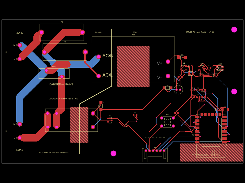 More from this authorabse/wifi-smart-switchThe AO3400A component models a small N-channel MOSFET in a SOT-23 package with drain, gate, and source pins, used for switching or amplification in electronic circuits.
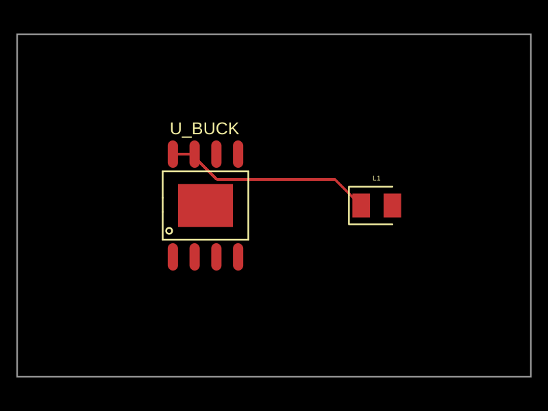 Similar packagemohan-bee/v7This code defines a surface-mount power regulator (LM5164DDAR) with specified pin labels and footprint information for use in a PCB design, incorporating 3D model references and silkscreen outlines.
 Discover something newShiboSoftwareDev/mspm0g3507-usb-c-dev-boardThe circuit assembles a USB-C port with integrated ESD protection, power regulation, UART interface, and microcontroller (MSPM0G3507) with supporting components for USB data lines, CC termination, I2C, SPI, reset circuitry, and indicator LEDs.