abse/boostxl-tmp107
This code defines a 6-pin electronic component with a specified footprint, 3D models, and pin labels, suitable for PCB design and visualization.
- Version
- 1.0.7
- License
- unset
- Stars
- 0
dist/index.js
import { jsx, jsxs } from 'react/jsx-runtime';
import objPath from '././assets/PZ254V_12_6P-73f3628b.obj';
import stepPath from '././assets/PZ254V_12_6P-10118318.step';
import objPath$1 from '././assets/SN74LVC1G07DBVR-14340306.obj';
import stepPath$1 from '././assets/SN74LVC1G07DBVR-48565a2c.step';
import objPath$2 from '././assets/SSQ_110_03_T_D-72062960.obj';
import stepPath$2 from '././assets/SSQ_110_03_T_D-62c92b4d.step';
import objPath$3 from '././assets/TMP107BIDR-918b31cc.obj';
import stepPath$3 from '././assets/TMP107BIDR-996ed896.step';

const pinLabels$3 = {
    pin1: ["pin1"],
    pin2: ["pin2"],
    pin3: ["pin3"],
    pin4: ["pin4"],
    pin5: ["pin5"],
    pin6: ["pin6"]
};
const PZ254V_12_6P = (props) => {
    return (jsx("chip", { pinLabels: pinLabels$3, supplierPartNumbers: {
            "jlcpcb": [
                "C492420"
            ]
        }, manufacturerPartNumber: "PZ254V-12-6P", footprint: jsxs("footprint", { children: [jsx("platedhole", { portHints: ["pin1"], pcbX: "-2.54mm", pcbY: "-1.27mm", outerDiameter: "1.6999966mm", holeDiameter: "1.1000232mm", shape: "circle" }), jsx("platedhole", { portHints: ["pin2"], pcbX: "-2.54mm", pcbY: "1.27mm", outerDiameter: "1.6999966mm", holeDiameter: "1.1000232mm", shape: "circle" }), jsx("platedhole", { portHints: ["pin3"], pcbX: "0mm", pcbY: "-1.27mm", outerDiameter: "1.6999966mm", holeDiameter: "1.1000232mm", shape: "circle" }), jsx("platedhole", { portHints: ["pin4"], pcbX: "0mm", pcbY: "1.27mm", outerDiameter: "1.6999966mm", holeDiameter: "1.1000232mm", shape: "circle" }), jsx("platedhole", { portHints: ["pin5"], pcbX: "2.54mm", pcbY: "-1.27mm", outerDiameter: "1.6999966mm", holeDiameter: "1.1000232mm", shape: "circle" }), jsx("platedhole", { portHints: ["pin6"], pcbX: "2.54mm", pcbY: "1.27mm", outerDiameter: "1.6999966mm", holeDiameter: "1.1000232mm", shape: "circle" }), jsx("silkscreenpath", { route: [{ "x": 4.039996999999971, "y": 2.5399999999999636 }, { "x": 4.039996999999971, "y": -2.5399999999999636 }] }), jsx("silkscreenpath", { route: [{ "x": -4.0399969999998575, "y": -2.5399999999999636 }, { "x": 4.039996999999971, "y": -2.5399999999999636 }] }), jsx("silkscreenpath", { route: [{ "x": -4.0399969999998575, "y": 2.5399999999999636 }, { "x": 4.039996999999971, "y": 2.5399999999999636 }] }), jsx("silkscreenpath", { route: [{ "x": -4.0399969999998575, "y": 0.007061199999952805 }, { "x": -1.2699999999999818, "y": 0.007061199999952805 }, { "x": -1.2699999999999818, "y": -2.5399999999999636 }] }), jsx("silkscreenpath", { route: [{ "x": -4.0399969999998575, "y": 2.5399999999999636 }, { "x": -4.0399969999998575, "y": -2.5399999999999636 }] }), jsx("silkscreentext", { text: "{NAME}", pcbX: "0mm", pcbY: "3.54mm", anchorAlignment: "center", fontSize: "1mm" }), jsx("courtyardoutline", { outline: [{ "x": -4.288599999999974, "y": 2.7899999999999636 }, { "x": 4.288600000000088, "y": 2.7899999999999636 }, { "x": 4.288600000000088, "y": -2.7899999999999636 }, { "x": -4.288599999999974, "y": -2.7899999999999636 }, { "x": -4.288599999999974, "y": 2.7899999999999636 }] })] }), cadModel: {
            objUrl: objPath,
            stepUrl: stepPath,
            pcbRotationOffset: 0,
            modelOriginPosition: { x: 2.545, y: -1.2700127000000703, z: -5999999999950489e-21 },
        }, ...props }));
};

const pinLabels$2 = {
    pin1: ["NC"],
    pin2: ["A"],
    pin3: ["GND"],
    pin4: ["Y"],
    pin5: ["VCC"],
};
const SN74LVC1G07DBVR = (props) => (jsx("chip", { pinLabels: pinLabels$2, supplierPartNumbers: { jlcpcb: ["C7829"] }, manufacturerPartNumber: "SN74LVC1G07DBVR", footprint: "dfn6_missing(5)_p0.95mm_w3.7002mm_pl1.1mm_pin1location(rightside,bottom)", cadModel: {
        objUrl: objPath$1,
        stepUrl: stepPath$1,
        pcbRotationOffset: 180,
        modelOriginPosition: { x: 0, y: -127e-7, z: -0.049083 },
    }, ...props }));

const pinLabels$1 = {
    pin1: ["pin1"],
    pin2: ["pin2"],
    pin3: ["pin3"],
    pin4: ["pin4"],
    pin5: ["pin5"],
    pin6: ["pin6"],
    pin7: ["pin7"],
    pin8: ["pin8"],
    pin9: ["pin9"],
    pin10: ["pin10"],
    pin11: ["pin11"],
    pin12: ["pin12"],
    pin13: ["pin13"],
    pin14: ["pin14"],
    pin15: ["pin15"],
    pin16: ["pin16"],
    pin17: ["pin17"],
    pin18: ["pin18"],
    pin19: ["pin19"],
    pin20: ["pin20"]
};
const SSQ_110_03_T_D = (props) => {
    return (jsx("chip", { pinLabels: pinLabels$1, supplierPartNumbers: {
            "jlcpcb": [
                "C5379997"
            ]
        }, manufacturerPartNumber: "SSQ-110-03-T-D", footprint: jsxs("footprint", { children: [jsx("platedhole", { portHints: ["pin20"], pcbX: "-11.43mm", pcbY: "1.27mm", outerDiameter: "1.530096mm", holeDiameter: "1.020064mm", shape: "circle" }), jsx("platedhole", { portHints: ["pin19"], pcbX: "-11.43mm", pcbY: "-1.27mm", outerDiameter: "1.530096mm", holeDiameter: "1.020064mm", shape: "circle" }), jsx("platedhole", { portHints: ["pin18"], pcbX: "-8.89mm", pcbY: "1.27mm", outerDiameter: "1.530096mm", holeDiameter: "1.020064mm", shape: "circle" }), jsx("platedhole", { portHints: ["pin17"], pcbX: "-8.89mm", pcbY: "-1.27mm", outerDiameter: "1.530096mm", holeDiameter: "1.020064mm", shape: "circle" }), jsx("platedhole", { portHints: ["pin16"], pcbX: "-6.35mm", pcbY: "1.27mm", outerDiameter: "1.530096mm", holeDiameter: "1.020064mm", shape: "circle" }), jsx("platedhole", { portHints: ["pin15"], pcbX: "-6.35mm", pcbY: "-1.27mm", outerDiameter: "1.530096mm", holeDiameter: "1.020064mm", shape: "circle" }), jsx("platedhole", { portHints: ["pin14"], pcbX: "-3.81mm", pcbY: "1.27mm", outerDiameter: "1.530096mm", holeDiameter: "1.020064mm", shape: "circle" }), jsx("platedhole", { portHints: ["pin13"], pcbX: "-3.81mm", pcbY: "-1.27mm", outerDiameter: "1.530096mm", holeDiameter: "1.020064mm", shape: "circle" }), jsx("platedhole", { portHints: ["pin12"], pcbX: "-1.27mm", pcbY: "1.27mm", outerDiameter: "1.530096mm", holeDiameter: "1.020064mm", shape: "circle" }), jsx("platedhole", { portHints: ["pin11"], pcbX: "-1.27mm", pcbY: "-1.27mm", outerDiameter: "1.530096mm", holeDiameter: "1.020064mm", shape: "circle" }), jsx("platedhole", { portHints: ["pin10"], pcbX: "1.27mm", pcbY: "1.27mm", outerDiameter: "1.530096mm", holeDiameter: "1.020064mm", shape: "circle" }), jsx("platedhole", { portHints: ["pin9"], pcbX: "1.27mm", pcbY: "-1.27mm", outerDiameter: "1.530096mm", holeDiameter: "1.020064mm", shape: "circle" }), jsx("platedhole", { portHints: ["pin8"], pcbX: "3.81mm", pcbY: "1.27mm", outerDiameter: "1.530096mm", holeDiameter: "1.020064mm", shape: "circle" }), jsx("platedhole", { portHints: ["pin7"], pcbX: "3.81mm", pcbY: "-1.27mm", outerDiameter: "1.530096mm", holeDiameter: "1.020064mm", shape: "circle" }), jsx("platedhole", { portHints: ["pin6"], pcbX: "6.35mm", pcbY: "1.27mm", outerDiameter: "1.530096mm", holeDiameter: "1.020064mm", shape: "circle" }), jsx("platedhole", { portHints: ["pin5"], pcbX: "6.35mm", pcbY: "-1.27mm", outerDiameter: "1.530096mm", holeDiameter: "1.020064mm", shape: "circle" }), jsx("platedhole", { portHints: ["pin4"], pcbX: "8.89mm", pcbY: "1.27mm", outerDiameter: "1.530096mm", holeDiameter: "1.020064mm", shape: "circle" }), jsx("platedhole", { portHints: ["pin3"], pcbX: "8.89mm", pcbY: "-1.27mm", outerDiameter: "1.530096mm", holeDiameter: "1.020064mm", shape: "circle" }), jsx("platedhole", { portHints: ["pin2"], pcbX: "11.43mm", pcbY: "1.27mm", outerDiameter: "1.530096mm", holeDiameter: "1.020064mm", shape: "circle" }), jsx("platedhole", { portHints: ["pin1"], pcbX: "11.43mm", pcbY: "-1.27mm", outerDiameter: "1.530096mm", holeDiameter: "1.020064mm", shape: "circle" }), jsx("silkscreenpath", { route: [{ "x": 12.955016, "y": -2.4749760000000833 }, { "x": -12.955016, "y": -2.4749760000000833 }, { "x": -12.955016, "y": 2.4749760000000833 }, { "x": 12.955016, "y": 2.4749760000000833 }, { "x": 12.955016, "y": -2.4749760000000833 }] }), jsx("silkscreentext", { text: "{NAME}", pcbX: "0.0127mm", pcbY: "3.4892mm", anchorAlignment: "center", fontSize: "1mm" }), jsx("courtyardoutline", { outline: [{ "x": -13.204000000000065, "y": 2.7391999999999825 }, { "x": 13.229399999999828, "y": 2.7391999999999825 }, { "x": 13.229399999999828, "y": -2.7391999999999825 }, { "x": -13.204000000000065, "y": -2.7391999999999825 }, { "x": -13.204000000000065, "y": 2.7391999999999825 }] })] }), cadModel: {
            objUrl: objPath$2,
            stepUrl: stepPath$2,
            pcbRotationOffset: 0,
            modelOriginPosition: { x: -12699999956566899e-21, y: -0.0049873000000433265, z: -10000000000509601e-21 },
        }, ...props }));
};

const pinLabels = {
    pin1: ["V_POS", "VCC"],
    pin2: ["R1"],
    pin3: ["IO1"],
    pin4: ["ALERT1"],
    pin5: ["GND"],
    pin6: ["ALERT2"],
    pin7: ["IO2"],
    pin8: ["R2"],
};
/**
 * Exact JLCPCB part C2870479. EasyEDA does not expose a symbol/model record for
 * this SKU, so the package model comes from pin-compatible C2870960. The
 * importer measured its SOIC-8 copper geometry at 100.00% IoU.
 */
const TMP107BIDR = (props) => (jsx("chip", { pinLabels: pinLabels, supplierPartNumbers: { jlcpcb: ["C2870479"] }, manufacturerPartNumber: "TMP107BIDR", footprint: "soic8_pillpads_w6.9999mm_pw0.588mm_pl1.8mm_pin1location(leftside,bottom)", cadModel: {
        objUrl: objPath$3,
        stepUrl: stepPath$3,
        pcbRotationOffset: 0,
        modelOriginPosition: { x: -127e-7, y: 0, z: 0 },
    }, ...props }));

const N = {
    V5: "net.V5",
    V33: "net.V33",
    GND: "net.GND",
    RXD: "net.UCA0RXD",
    TXD: "net.UCA0TXD",
    TX_OD: "net.TX_OD",
    TX_R: "net.TX_R",
    BUS: "net.TMP_BUS",
    ALERT1: "net.ALERT1",
    ALERT2: "net.ALERT2",
    IO12: "net.IO1_2",
    IO13: "net.IO1_3",
    IO14: "net.IO1_4",
};
const HEADER_SCH_PIN_STYLE = {
    pin1: { marginTop: "0.05mm", marginBottom: "0.05mm" },
    pin2: { marginTop: "0.05mm", marginBottom: "0.05mm" },
    pin3: { marginTop: "0.05mm", marginBottom: "0.05mm" },
    pin4: { marginTop: "0.05mm", marginBottom: "0.05mm" },
    pin5: { marginTop: "0.05mm", marginBottom: "0.05mm" },
    pin6: { marginTop: "0.05mm", marginBottom: "0.05mm" },
    pin7: { marginTop: "0.05mm", marginBottom: "0.05mm" },
    pin8: { marginTop: "0.05mm", marginBottom: "0.05mm" },
    pin9: { marginTop: "0.05mm", marginBottom: "0.05mm" },
    pin10: { marginTop: "0.05mm", marginBottom: "0.05mm" },
    pin11: { marginTop: "0.05mm", marginBottom: "0.05mm" },
    pin12: { marginTop: "0.05mm", marginBottom: "0.05mm" },
    pin13: { marginTop: "0.05mm", marginBottom: "0.05mm" },
    pin14: { marginTop: "0.05mm", marginBottom: "0.05mm" },
    pin15: { marginTop: "0.05mm", marginBottom: "0.05mm" },
    pin16: { marginTop: "0.05mm", marginBottom: "0.05mm" },
    pin17: { marginTop: "0.05mm", marginBottom: "0.05mm" },
    pin18: { marginTop: "0.05mm", marginBottom: "0.05mm" },
    pin19: { marginTop: "0.05mm", marginBottom: "0.05mm" },
    pin20: { marginTop: "0.05mm", marginBottom: "0.05mm" },
};
const TMP107_SCH_PIN_STYLE = {
    pin1: { marginTop: "0.075mm", marginBottom: "0.075mm" },
    pin2: { marginTop: "0.075mm", marginBottom: "0.075mm" },
    pin3: { marginTop: "0.075mm", marginBottom: "0.075mm" },
    pin4: { marginTop: "0.075mm", marginBottom: "0.075mm" },
    pin5: { marginTop: "0.075mm", marginBottom: "0.075mm" },
    pin6: { marginTop: "0.075mm", marginBottom: "0.075mm" },
    pin7: { marginTop: "0.075mm", marginBottom: "0.075mm" },
    pin8: { marginTop: "0.075mm", marginBottom: "0.075mm" },
};
const SHUNT_HEADER_SCH_PIN_STYLE = {
    pin1: { marginTop: "0.15mm", marginBottom: "0.15mm" },
    pin2: { marginTop: "0.15mm", marginBottom: "0.15mm" },
    pin3: { marginTop: "0.15mm", marginBottom: "0.15mm" },
    pin4: { marginTop: "0.15mm", marginBottom: "0.15mm" },
    pin5: { marginTop: "0.15mm", marginBottom: "0.15mm" },
    pin6: { marginTop: "0.15mm", marginBottom: "0.15mm" },
};
function Circuit() {
    return (jsxs("board", { name: "BOOSTXL_TMP107", width: "53.34mm", height: "40.64mm", outline: [
            { x: -26.67, y: -20.32 },
            { x: 26.67, y: -20.32 },
            { x: 26.67, y: 20.32 },
            { x: -26.67, y: 20.32 },
        ], solderMaskColor: "red", silkscreenColor: "white", defaultTraceWidth: "0.2mm", minViaHoleDiameter: "0.3mm", minViaPadDiameter: "0.45mm", autorouter: {
            preset: "auto_local",
            local: true,
            traceClearance: "0.15mm",
        }, autorouterEffortLevel: "2x", children: [jsx("schematicsheet", { name: "BOOSTXL-TMP107 Complete Schematic", displayName: "BOOSTXL-TMP107 Complete Schematic", sheetIndex: 1 }), jsxs("group", { name: "COMPLETE_SCHEMATIC", schSheetName: "BOOSTXL-TMP107 Complete Schematic", schX: 0, schY: 0, pcbX: 0, pcbY: 0, schMaxTraceDistance: "1.2mm", schTraceAutoLabelEnabled: true, children: [jsx("schematicsection", { name: "TI_MHR035_FUNCTIONAL_CIRCUIT", displayName: "TI MHR035 Rev A functional circuit", sectionTitleFontSize: "0.18mm" }), jsx(SSQ_110_03_T_D, { name: "J1", layer: "bottom", schSectionName: "TI_MHR035_FUNCTIONAL_CIRCUIT", schX: -9.5, schY: 7.2, schWidth: "5.2mm", schHeight: "3mm", schPinStyle: HEADER_SCH_PIN_STYLE, schPinArrangement: {
                            leftSide: [1, 3, 5, 7, 9, 11, 13, 15, 17, 19],
                            rightSide: [2, 4, 6, 8, 10, 12, 14, 16, 18, 20],
                        }, pcbX: -20.32, pcbY: 7.0, pcbRotation: 90, noConnect: ["pin3", "pin6", "pin8", "pin9", "pin10", "pin11", "pin12", "pin13", "pin14", "pin15", "pin16", "pin17", "pin18", "pin19", "pin20"], connections: {
                            pin1: N.V33,
                            pin2: N.V5,
                            pin4: N.GND,
                            pin5: N.RXD,
                            pin7: N.TXD,
                        } }), jsx(SSQ_110_03_T_D, { name: "J2", layer: "bottom", schSectionName: "TI_MHR035_FUNCTIONAL_CIRCUIT", schX: -0.5, schY: 6.9, schWidth: "5.2mm", schHeight: "3mm", schPinStyle: HEADER_SCH_PIN_STYLE, schPinArrangement: {
                            leftSide: [1, 3, 5, 7, 9, 11, 13, 15, 17, 19],
                            rightSide: [2, 4, 6, 8, 10, 12, 14, 16, 18, 20],
                        }, pcbX: 20.32, pcbY: 7.0, pcbRotation: 90, noConnect: ["pin2", "pin3", "pin4", "pin5", "pin6", "pin7", "pin8", "pin9", "pin10", "pin11", "pin13", "pin14", "pin15", "pin16", "pin17", "pin19", "pin20"], connections: {
                            pin1: N.GND,
                            pin12: N.ALERT1,
                            pin18: N.ALERT2,
                        } }), jsx("schematictext", { text: "Install one shunt: 1-2 DRV, 3-4 RES, or 5-6 SHORT", schX: -13.7, schY: 1.7, fontSize: 0.2, anchor: "center_left" }), jsx(SN74LVC1G07DBVR, { name: "U1", schSectionName: "TI_MHR035_FUNCTIONAL_CIRCUIT", noSchematicRepresentation: true, pcbX: -11.7, pcbY: 1.4, noConnect: ["NC"], connections: {
                            A: N.TXD,
                            GND: N.GND,
                            Y: N.TX_OD,
                            VCC: N.V33,
                        } }), jsx("schematicsymbol", { name: "U1_BUFFER", displayName: "U1", chipRef: ".U1", symbolName: "opamp_with_power", schSectionName: "TI_MHR035_FUNCTIONAL_CIRCUIT", schX: -11.5, schY: -3, connections: {
                            inp1: ".U1 > .A",
                            inp2: ".U1 > .NC",
                            out: ".U1 > .Y",
                            "V+": ".U1 > .VCC",
                            "V-": ".U1 > .GND",
                        } }), jsx("capacitor", { name: "C1", schSectionName: "TI_MHR035_FUNCTIONAL_CIRCUIT", schX: -11.5, schY: -0.7, schRotation: "0deg", manufacturerPartNumber: "GRM188R71E104KA01D", supplierPartNumbers: { jlcpcb: ["C77050"] }, capacitance: "0.1uF", footprint: "0603", pcbX: -16.1, pcbY: 1.0, pcbRotation: 90, connections: { pin1: N.V33, pin2: N.GND } }), jsx("resistor", { name: "R1", schSectionName: "TI_MHR035_FUNCTIONAL_CIRCUIT", schX: -8.2, schY: -2.1, schRotation: "0deg", manufacturerPartNumber: "0603WAF3301T5E", supplierPartNumbers: { jlcpcb: ["C22978"] }, resistance: "3.3kohm", footprint: "0603", pcbX: -15, pcbY: 5.4, connections: { pin1: N.V33, pin2: N.TX_OD } }), jsx("resistor", { name: "R2", schSectionName: "TI_MHR035_FUNCTIONAL_CIRCUIT", schX: -8.2, schY: -5.2, manufacturerPartNumber: "CQ03WAF1002T5E", supplierPartNumbers: { jlcpcb: ["C516551"] }, resistance: "10kohm", footprint: "0603", pcbX: -7.6, pcbY: 5.4, connections: { pin1: N.TXD, pin2: N.TX_R } }), jsx(PZ254V_12_6P, { name: "J3", schSectionName: "TI_MHR035_FUNCTIONAL_CIRCUIT", schX: -5.4, schY: -3.6, schWidth: "2.4mm", schHeight: "1.5mm", schPinStyle: SHUNT_HEADER_SCH_PIN_STYLE, schPinArrangement: { leftSide: [1, 3, 5], rightSide: [2, 4, 6] }, pcbX: -8.6, pcbY: 11.3, connections: {
                            pin1: N.TX_OD,
                            pin2: N.BUS,
                            pin3: N.TX_R,
                            pin4: N.BUS,
                            pin5: N.TXD,
                            pin6: N.BUS,
                        } }), jsx(TMP107BIDR, { name: "U2", schSectionName: "TI_MHR035_FUNCTIONAL_CIRCUIT", schX: -0.5, schY: -3, schWidth: "2.5mm", schHeight: "2.9mm", schPinStyle: TMP107_SCH_PIN_STYLE, schPinArrangement: {
                            leftSide: [1, 3, 7],
                            rightSide: [2, 8, 4, 6, 5],
                        }, pcbX: 3.4, pcbY: 9.9, pcbRotation: 90, connections: {
                            V_POS: N.V33,
                            R1: N.V33,
                            IO1: N.BUS,
                            ALERT1: N.ALERT1,
                            GND: N.GND,
                            ALERT2: N.ALERT2,
                            IO2: N.IO12,
                            R2: N.V33,
                        } }), jsx("capacitor", { name: "C2", schSectionName: "TI_MHR035_FUNCTIONAL_CIRCUIT", schX: -0.5, schY: -0.7, schRotation: "0deg", manufacturerPartNumber: "GRM188R71E104KA01D", supplierPartNumbers: { jlcpcb: ["C77050"] }, capacitance: "0.1uF", footprint: "0603", pcbX: 0.8, pcbY: 14.4, connections: { pin1: N.V33, pin2: N.GND } }), jsx(TMP107BIDR, { name: "U3", schSectionName: "TI_MHR035_FUNCTIONAL_CIRCUIT", schX: 5, schY: -2.8, schWidth: "2.5mm", schHeight: "2.9mm", schPinStyle: TMP107_SCH_PIN_STYLE, schPinArrangement: {
                            leftSide: [1, 3, 7],
                            rightSide: [2, 8, 4, 6, 5],
                        }, pcbX: 4.5, pcbY: -15.7, pcbRotation: 0, noConnect: ["ALERT1", "ALERT2"], connections: {
                            V_POS: N.V33,
                            R1: N.V33,
                            IO1: N.IO12,
                            GND: N.GND,
                            IO2: N.IO13,
                            R2: N.V33,
                        } }), jsx("capacitor", { name: "C3", schSectionName: "TI_MHR035_FUNCTIONAL_CIRCUIT", schX: 5, schY: 0, schRotation: "0deg", manufacturerPartNumber: "GRM188R71E104KA01D", supplierPartNumbers: { jlcpcb: ["C77050"] }, capacitance: "0.1uF", footprint: "0603", pcbX: -0.2, pcbY: -16.8, pcbRotation: 90, connections: { pin1: N.V33, pin2: N.GND } }), jsx(TMP107BIDR, { name: "U4", schSectionName: "TI_MHR035_FUNCTIONAL_CIRCUIT", schX: 10.5, schY: -2.8, schWidth: "2.5mm", schHeight: "2.9mm", schPinStyle: TMP107_SCH_PIN_STYLE, schPinArrangement: {
                            leftSide: [1, 3, 7],
                            rightSide: [2, 8, 4, 6, 5],
                        }, pcbX: 19.1, pcbY: -15.7, pcbRotation: 0, noConnect: ["ALERT1", "ALERT2"], connections: {
                            V_POS: N.V33,
                            R1: N.V33,
                            IO1: N.IO13,
                            GND: N.GND,
                            IO2: N.IO14,
                            R2: N.V33,
                        } }), jsx("capacitor", { name: "C4", schSectionName: "TI_MHR035_FUNCTIONAL_CIRCUIT", schX: 10.5, schY: 0, schRotation: "270deg", manufacturerPartNumber: "GRM188R71E104KA01D", supplierPartNumbers: { jlcpcb: ["C77050"] }, capacitance: "0.1uF", footprint: "0603", pcbX: 15.4, pcbY: -14.1, pcbRotation: 90, connections: { pin1: N.V33, pin2: N.GND } }), jsx("schematicrect", { schX: 5, schY: -2.2, width: "4.4mm", height: "7.2mm", strokeWidth: "0.03mm", color: "#555555" }), jsx("schematictext", { text: "layout 3 pin coupon board as breakaway", schX: 5, schY: 1.05, fontSize: 0.14, anchor: "center" }), jsx("schematicrect", { schX: 10.5, schY: -2.2, width: "4.4mm", height: "7.2mm", strokeWidth: "0.03mm", color: "#555555" }), jsx("schematictext", { text: "layout 3 pin coupon board as breakaway", schX: 10.5, schY: 1.05, fontSize: 0.14, anchor: "center" })] }), jsx("platedhole", { name: "MAIN_V33", shape: "circle", outerDiameter: "1.8mm", holeDiameter: "0.9mm", pcbX: -15.24, pcbY: -5.1, connectsTo: N.V33 }), jsx("platedhole", { name: "MAIN_IO1", shape: "circle", outerDiameter: "1.8mm", holeDiameter: "0.9mm", pcbX: -12.7, pcbY: -5.1, connectsTo: N.IO12 }), jsx("platedhole", { name: "MAIN_GND", shape: "circle", outerDiameter: "1.8mm", holeDiameter: "0.9mm", pcbX: -10.16, pcbY: -5.1, connectsTo: N.GND }), jsx("platedhole", { name: "U3_IN_V33", shape: "circle", outerDiameter: "1.8mm", holeDiameter: "0.9mm", pcbX: -1.9, pcbY: -11.5, connectsTo: N.V33 }), jsx("platedhole", { name: "U3_IN_IO1", shape: "circle", outerDiameter: "1.8mm", holeDiameter: "0.9mm", pcbX: -1.9, pcbY: -15.5, connectsTo: N.IO12 }), jsx("platedhole", { name: "U3_IN_GND", shape: "circular_hole_with_rect_pad", holeDiameter: "0.9mm", rectPadWidth: "1.8mm", rectPadHeight: "1.8mm", pcbX: -1.9, pcbY: -19, connectsTo: N.GND }), jsx("platedhole", { name: "U3_OUT_V33", shape: "circle", outerDiameter: "1.8mm", holeDiameter: "0.9mm", pcbX: 10.2, pcbY: -11.5, connectsTo: N.V33 }), jsx("platedhole", { name: "U3_OUT_IO2", shape: "circle", outerDiameter: "1.8mm", holeDiameter: "0.9mm", pcbX: 10.2, pcbY: -15.5, connectsTo: N.IO13 }), jsx("platedhole", { name: "U3_OUT_GND", shape: "circular_hole_with_rect_pad", holeDiameter: "0.9mm", rectPadWidth: "1.8mm", rectPadHeight: "1.8mm", pcbX: 10.2, pcbY: -19, connectsTo: N.GND }), jsx("platedhole", { name: "U4_IN_V33", shape: "circle", outerDiameter: "1.8mm", holeDiameter: "0.9mm", pcbX: 13.9, pcbY: -11.5, connectsTo: N.V33 }), jsx("platedhole", { name: "U4_IN_IO1", shape: "circle", outerDiameter: "1.8mm", holeDiameter: "0.9mm", pcbX: 13.9, pcbY: -15.5, connectsTo: N.IO13 }), jsx("platedhole", { name: "U4_IN_GND", shape: "circular_hole_with_rect_pad", holeDiameter: "0.9mm", rectPadWidth: "1.8mm", rectPadHeight: "1.8mm", pcbX: 13.9, pcbY: -19, connectsTo: N.GND }), jsx("platedhole", { name: "U4_OUT_V33", shape: "circle", outerDiameter: "1.8mm", holeDiameter: "0.9mm", pcbX: 25.4, pcbY: -11.5, connectsTo: N.V33 }), jsx("platedhole", { name: "U4_OUT_IO2", shape: "circle", outerDiameter: "1.8mm", holeDiameter: "0.9mm", pcbX: 25.4, pcbY: -15.5, connectsTo: N.IO14 }), jsx("platedhole", { name: "U4_OUT_GND", shape: "circular_hole_with_rect_pad", holeDiameter: "0.9mm", rectPadWidth: "1.8mm", rectPadHeight: "1.8mm", pcbX: 25.4, pcbY: -19, connectsTo: N.GND }), jsx("cutout", { name: "BREAK_SLOT_1", shape: "rect", width: "4.2mm", height: "0.75mm", pcbX: -23.6, pcbY: -9.5 }), jsx("cutout", { name: "BREAK_SLOT_2", shape: "rect", width: "4.2mm", height: "0.75mm", pcbX: -18.1, pcbY: -9.5 }), jsx("cutout", { name: "BREAK_SLOT_3", shape: "rect", width: "4.2mm", height: "0.75mm", pcbX: -12.6, pcbY: -9.5 }), jsx("cutout", { name: "BREAK_SLOT_4", shape: "rect", width: "4.2mm", height: "0.75mm", pcbX: -7.1, pcbY: -9.5 }), jsx("cutout", { name: "BREAK_SLOT_5", shape: "rect", width: "4.2mm", height: "0.75mm", pcbX: -1.6, pcbY: -9.5 }), jsx("cutout", { name: "BREAK_SLOT_6", shape: "rect", width: "4.2mm", height: "0.75mm", pcbX: 3.9, pcbY: -9.5 }), jsx("cutout", { name: "BREAK_SLOT_7", shape: "rect", width: "4.2mm", height: "0.75mm", pcbX: 9.4, pcbY: -9.5 }), jsx("cutout", { name: "BREAK_SLOT_8", shape: "rect", width: "4.2mm", height: "0.75mm", pcbX: 14.9, pcbY: -9.5 }), jsx("cutout", { name: "BREAK_SLOT_9", shape: "rect", width: "4.2mm", height: "0.75mm", pcbX: 20.4, pcbY: -9.5 }), jsx("cutout", { name: "BREAK_SLOT_10", shape: "rect", width: "2.2mm", height: "0.75mm", pcbX: 24.9, pcbY: -9.5 }), jsx("cutout", { name: "NODE_2_LEFT_SLOT_1", shape: "rect", width: "0.75mm", height: "2.8mm", pcbX: -4.35, pcbY: -11.3 }), jsx("cutout", { name: "NODE_2_LEFT_SLOT_2", shape: "rect", width: "0.75mm", height: "2.8mm", pcbX: -4.35, pcbY: -14.6 }), jsx("cutout", { name: "NODE_2_LEFT_SLOT_3", shape: "rect", width: "0.75mm", height: "2.8mm", pcbX: -4.35, pcbY: -17.9 }), jsx("cutout", { name: "NODE_DIVIDER_SLOT_1", shape: "rect", width: "0.75mm", height: "2.8mm", pcbX: 12.05, pcbY: -11.3 }), jsx("cutout", { name: "NODE_DIVIDER_SLOT_2", shape: "rect", width: "0.75mm", height: "2.8mm", pcbX: 12.05, pcbY: -14.6 }), jsx("cutout", { name: "NODE_DIVIDER_SLOT_3", shape: "rect", width: "0.75mm", height: "2.8mm", pcbX: 12.05, pcbY: -17.9 }), jsx("copperpour", { name: "GND_BOTTOM", layer: "bottom", connectsTo: N.GND, padMargin: "0.25mm", traceMargin: "0.2mm", boardEdgeMargin: "0.3mm" }), jsx("silkscreentext", { text: "BOOSTXL-TMP107", pcbX: 0, pcbY: 18.2, fontSize: "1.2mm" }), jsx("silkscreentext", { text: "1-2 DRV   3-4 RES   5-6 SHORT", pcbX: -8.6, pcbY: 16.6, fontSize: "0.42mm" }), jsx("silkscreentext", { text: "3V3", pcbX: -25.1, pcbY: 15.2, fontSize: "0.65mm" }), jsx("silkscreentext", { text: "RXD", pcbX: -25.1, pcbY: 11.2, fontSize: "0.65mm" }), jsx("silkscreentext", { text: "TXD", pcbX: -25.1, pcbY: 8.3, fontSize: "0.65mm" }), jsx("silkscreentext", { text: "ALERT1", pcbX: 13.5, pcbY: 1.4, fontSize: "0.65mm" }), jsx("silkscreentext", { text: "ALERT2", pcbX: 13.5, pcbY: -0.8, fontSize: "0.65mm" }), jsx("silkscreentext", { text: "V+   IO1   GND", pcbX: -12.7, pcbY: -7.2, fontSize: "0.55mm" }), jsx("silkscreentext", { text: "TMP107 NODE 2", pcbX: 4.5, pcbY: -10.7, fontSize: "0.42mm" }), jsx("silkscreentext", { text: "TMP107 NODE 3", pcbX: 19.1, pcbY: -10.7, fontSize: "0.42mm" }), jsx("silkscreentext", { text: "TMP107", pcbX: 7.6, pcbY: -15.7, pcbRotation: 90, fontSize: "0.55mm" }), jsx("silkscreentext", { text: "TMP107", pcbX: 23.2, pcbY: -15.7, pcbRotation: 90, fontSize: "0.55mm" }), jsx("silkscreentext", { text: "MHR035 REV A RECONSTRUCTION", pcbX: 0, pcbY: -7.7, fontSize: "0.45mm" })] }));
}

export { Circuit as default };
Related Packages
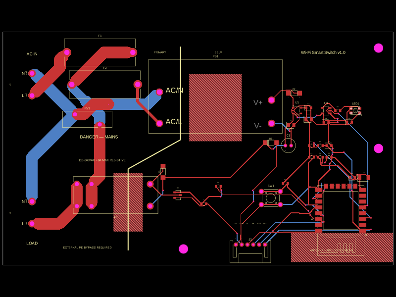 More from this authorabse/wifi-smart-switchThe AO3400A component models a small N-channel MOSFET in a SOT-23 package with drain, gate, and source pins, used for switching or amplification in electronic circuits.
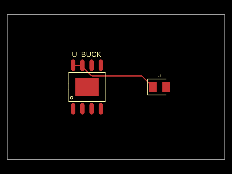 Similar packagemohan-bee/v7This code defines a surface-mount power regulator (LM5164DDAR) with specified pin labels and footprint information for use in a PCB design, incorporating 3D model references and silkscreen outlines.
 Discover something newShiboSoftwareDev/mspm0g3507-usb-c-dev-boardThe circuit assembles a USB-C port with integrated ESD protection, power regulation, UART interface, and microcontroller (MSPM0G3507) with supporting components for USB data lines, CC termination, I2C, SPI, reset circuitry, and indicator LEDs.