ShiboSoftwareDev/nema8-20mm-pd-mini-controller
A 20 mm four-layer USB‑C PD 9 V NEMA8 stepper-driver board using CH224K power negotiation/protection and a TMC2209 with current sensing, motor connector, and STEP/DIR/UART control test points.
- Version
- 1.0.2
- License
- unset
- Stars
- 0
index.circuit.tsx
PCB
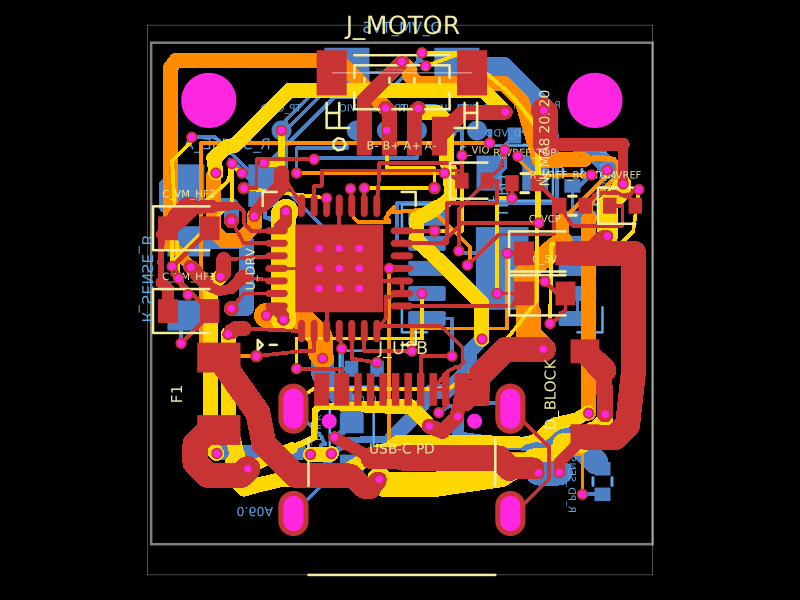
Schematic

import { Fragment } from "react"
import type { FanoutTracePath } from "@tscircuit/props"
import { BM04B_SRSS_TB_LF__SN_ } from "./imports/BM04B_SRSS_TB_LF__SN_"
import { BSMD1206_110_16V } from "./imports/BSMD1206_110_16V"
import { CH224K } from "./imports/CH224K"
import { PMEG6020ELRX } from "./imports/PMEG6020ELRX"
import { PT1206FR_7W0R33L } from "./imports/PT1206FR_7W0R33L"
import { SMAJ12A } from "./imports/SMAJ12A"
import { TMC2209_LA_T } from "./imports/TMC2209_LA_T"
import { TYPE_C_31_M_12 } from "./imports/TYPE_C_31_M_12"

const resistorParts: Record<string, string> = {
  "27": "C25100", "1k": "C11702", "5.1k": "C25905", "6.8k": "C25907", "10k": "C25744",
  "12k": "C25752", "47k": "C25792", "56k": "C25794", "100k": "C25741", "270k": "C25770",
}

const capacitorParts: Record<string, { part: string; footprint: string; voltage: string }> = {
  "22nF_50V": { part: "C1532", footprint: "0402", voltage: "50V" },
  "100nF": { part: "C1525", footprint: "0402", voltage: "16V" },
  "100nF_50V": { part: "C14663", footprint: "0603", voltage: "50V" },
  "1uF_50V": { part: "C28323", footprint: "0805", voltage: "50V" },
  "2.2uF": { part: "C23630", footprint: "0603", voltage: "16V" },
  "10uF_25V": { part: "C96446", footprint: "0603", voltage: "25V" },
}

const R = ({ name, resistance, ...props }: any) => (
  <resistor name={name} resistance={resistance} footprint="0402"
    schSheetName="main"
    supplierPartNumbers={{ jlcpcb: [resistorParts[resistance]] }} {...props} />
)

const C = ({ name, value, ...props }: any) => {
  const item = capacitorParts[value]
  return <capacitor name={name} capacitance={value.replace("_50V", "").replace("_25V", "")}
    footprint={item.footprint} maxVoltageRating={item.voltage}
    schSheetName="main"
    maxDecouplingTraceLength="100mm"
    supplierPartNumbers={{ jlcpcb: [item.part] }} {...props} />
}

const nets = [
  "GND", "VBUS_RAW", "VBUS_FUSED", "VM", "VIO", "USB_CC1", "USB_CC2",
  "PD_VDD", "PD_SENSE", "PD_CFG1",
  "STEP", "DIR", "ENN", "UART_DRV", "V5_DRV",
  "VREF", "CP_HI", "CP_LO", "VCP", "SENSE_A", "SENSE_B", "MOTOR_B_NEG",
  "MOTOR_B_POS", "MOTOR_A_POS", "MOTOR_A_NEG",
] as const

const netWidths: Partial<Record<(typeof nets)[number], string>> = {
  VBUS_RAW: "1mm", VBUS_FUSED: "1mm", VM: "1mm", SENSE_A: "0.6mm", SENSE_B: "0.6mm",
  MOTOR_B_NEG: "0.6mm", MOTOR_B_POS: "0.6mm", MOTOR_A_POS: "0.6mm", MOTOR_A_NEG: "0.6mm",
}
const thermalViaOffsets = [-0.8, 0, 0.8] as const
const driverY = 1.0
const driverSelector = ".U_DRV"

const topEscape = (
  port: string,
  points: Array<[number, number]>,
): FanoutTracePath => ({
  connection: `.U_DRV > .${port}`,
  route: points.map(([x, y]) => ({ route_type: "wire", x, y, width: 0.15, layer: "top" })),
})

const innerEscape = (
  port: string,
  start: [number, number],
  viaStart: [number, number],
  viaEnd: [number, number],
  layer: "inner1" | "inner2",
): FanoutTracePath => ({
  connection: `.U_DRV > .${port}`,
  route: [
    { route_type: "wire", x: start[0], y: start[1], width: 0.15, layer: "top" },
    { route_type: "wire", x: viaStart[0], y: viaStart[1], width: 0.15, layer: "top" },
    { route_type: "via", x: viaStart[0], y: viaStart[1], from_layer: "top", to_layer: layer,
      via_diameter: 0.45, via_hole_diameter: 0.3 },
    { route_type: "wire", x: viaStart[0], y: viaStart[1], width: 0.15, layer },
    { route_type: "wire", x: viaEnd[0], y: viaEnd[1], width: 0.15, layer },
    { route_type: "via", x: viaEnd[0], y: viaEnd[1], from_layer: layer, to_layer: "top",
      via_diameter: 0.45, via_hole_diameter: 0.3 },
    { route_type: "wire", x: viaEnd[0], y: viaEnd[1], width: 0.15, layer: "top" },
  ],
})

/* Deterministic exits keep the default autorouter away from the 0.5 mm-pitch
 * QFN pin field. Motor, sense and supply paths leave the fanout on an outer
 * layer; only low-current STEP/DIR/STDBY signals use the internal layers. */
const driverFanoutTracePaths: FanoutTracePath[] = [
  topEscape("OB2", [[-1.5, -2.5], [-3.8, -2.4]]),
  topEscape("SPREAD", [[1.5, -2.5], [3.8, -2.4]]),
  topEscape("5VOUT", [[2.5, -1.5], [3.8, -1.5]]),
  topEscape("MS1_AD0", [[2.5, -1], [3.8, -1]]),
  topEscape("PDN_UART", [[2.5, 1.5], [3.8, 1.5]]),
  topEscape("VCC_IO", [[1.5, 2.5], [1.6, 3.8]]),
  innerEscape("STEP", [1, 2.5], [1, 3.2], [3.8, 3.2], "inner2"),
  topEscape("VREF", [[0.5, 2.5], [0.35, 3.8]]),
  innerEscape("DIR", [-0.5, 2.5], [-0.5, 2.8], [-3.8, 3.2], "inner2"),
  topEscape("OA2", [[-1.5, 2.5], [-1.6, 3.8]]),
  topEscape("VS2", [[-2.5, 1.5], [-3.8, 1.6]]),
  topEscape("BRA", [[-2.5, 1], [-3.8, 1]]),
  topEscape("OA1", [[-2.5, 0.5], [-3.8, 0.35]]),
  topEscape("OB1", [[-2.5, -0.5], [-3.8, -0.35]]),
  topEscape("BRB", [[-2.5, -1], [-3.8, -1]]),
  topEscape("VS1", [[-2.5, -1.5], [-3.8, -1.6]]),
]

export default function Nema8TwentyMillimeterController() {
  return (
    <board width="20mm" height="20mm" layers={4} thickness="1.6mm"
      fabricatorPreset="jlcpcb_standard_20260912"
      autorouterEffortLevel="10x"
      minTraceWidth="0.15mm" minTraceToPadEdgeClearance="0.1mm"
      minViaEdgeToPadEdgeClearance="0.1mm" minViaHoleEdgeToViaHoleEdgeClearance="0.2mm"
      minPlatedHoleDrillEdgeToDrillEdgeClearance="0.3mm" minPadEdgeToPadEdgeClearance="0.1mm"
      minBoardEdgeClearance="0.17mm" minViaHoleDiameter="0.3mm" minViaPadDiameter="0.45mm"
      isViaInPadAllowed
      autorouter={{ preset: "default", allowViaInPad: false, traceClearance: "0.2mm" }}
      pcbStyle={{ viaHoleDiameter: "0.3mm", viaPadDiameter: "0.45mm" }}>
      <schematicsection name="Power" displayName="USB-C / USB-PD power" />
      <schematicsection name="Control" displayName="External STEP/DIR/UART control" />
      <schematicsection name="Driver" displayName="TMC2209 motor stage" />
      <schematicsheet name="main" displayName="NEMA8 20 mm stepper driver" sheetSize="A4">
        <schematictext schX={-18} schY={12.7} anchor="top_left" fontSize={0.2}
          text="USB-C PD INPUT — U_PD (CH224K) negotiates a fixed 9 V contract." />
        <schematictext schX={-12} schY={9.5} anchor="top_left" fontSize={0.2}
          text="PROTECTION — F1 1.1 A resettable fuse, reverse-current diode, 12 V TVS, and 10 uF/25 V bulk capacitor." />
        <schematictext schX={0} schY={10} anchor="top_left" fontSize={0.2}
          text="STEPPER STAGE — U_DRV is a TMC2209 stepper driver." />
        <schematictext schX={0} schY={9.5} anchor="top_left" fontSize={0.2}
          text="Motor: StepperOnline 8HS15-0604S, 0.60 A/phase, 11 ohm, 5.5 mH." />
        <schematictext schX={-9} schY={-7.7} anchor="top_left" fontSize={0.2}
          text="HOST I/O — External VIO, STEP, DIR, ENN, UART, and GND." />
        <schematictext schX={-9} schY={-8.2} anchor="top_left" fontSize={0.2}
          text="MOTOR I/O — B-, B+, A+, A-." />
      </schematicsheet>
      <schematicsheet name="implementation" displayName="PCB routing breakouts" sheetSize="A4">
        <schematictext schX={-18} schY={13} anchor="top_left" fontSize={0.2}
          text="PCB ROUTING BREAKOUTS — Internal test pads split physical routes; functional interfaces are documented on the main sheet." />
      </schematicsheet>
      {nets.map((name) => <Fragment key={name}><net name={name} nominalTraceWidth={netWidths[name]} /></Fragment>)}
      <TYPE_C_31_M_12 name="J_USB" pcbX={0} pcbY={-6.0} pcbRotation={0}
        schSectionName="Power" schSheetName="main" schX={-15} schY={7}
        noConnect={["SBU1", "SBU2", "DP1", "DP2", "DN1", "DN2"]}
        connections={{ EH1: "net.GND", EH2: "net.GND", EH3: "net.GND", EH4: "net.GND",
          GND1: "net.GND", GND2: "net.GND",
          VBUS1: "net.VBUS_RAW", VBUS2: "net.VBUS_RAW" }} />
      <CH224K name="U_PD" layer="bottom" pcbX={4.0} pcbY={1.0} pcbRotation={90}
        schSectionName="Power" schSheetName="main" schX={-13.78} schY={11} schWidth={3} schHeight={3}
        noConnect={["CFG2", "CFG3", "PG"]}
        connections={{ VDD: "net.PD_VDD", GND: "net.GND", VBUS: "net.PD_SENSE" }} />
      <R name="R_PD_VDD" resistance="1k" layer="bottom" pcbX={6.8} pcbY={4.8} pcbRotation={90}
        schSectionName="Power" schX={-17} schY={11.5}
        connections={{ pin1: "net.VBUS_RAW", pin2: "net.PD_VDD" }} />
      <C name="C_PD_VDD" value="1uF_50V" layer="bottom" pcbX={4.4} pcbY={4.8}
        schSectionName="Power" schX={-17} schY={10}
        connections={{ pin1: "net.PD_VDD", pin2: "net.GND" }} />
      <R name="R_PD_SENSE" resistance="10k" layer="bottom" pcbX={8.0} pcbY={-7.5} pcbRotation={90}
        schSectionName="Power" schX={-9.72} schY={11.5}
        connections={{ pin1: "net.VBUS_RAW", pin2: "net.PD_SENSE" }} />
      <R name="R_PD_SET_9V" resistance="6.8k" layer="bottom" pcbX={5.0} pcbY={6.3}
        schSectionName="Power" schX={-7.5} schY={11.5}
        connections={{ pin2: "net.GND" }} />
      <trace name="PD_CC1_ROUTE" from=".J_USB > .CC1" to=".U_PD > .CC1"
        thickness="0.15mm" maxViaCount={2} pcbPathRelativeTo=".J_USB > .CC1" pcbPath={[
          { x: -2.4, y: 3.0 }, { x: -4.2, y: 3.0 },
          { x: -4.2, y: 3.0, via: true, fromLayer: "top", toLayer: "inner2" },
          { x: -4.2, y: 3.0 }, { x: -4.2, y: 4.2 },
          { x: 0.8, y: 4.2 }, { x: 0.8, y: 6.0 },
          { x: 0.8, y: 6.0, via: true, fromLayer: "inner2", toLayer: "bottom" },
          { x: 0.8, y: 6.0 },
        ]} />
      <trace name="PD_CC2_ROUTE" from=".J_USB > .CC2" to=".U_PD > .CC2"
        thickness="0.15mm" maxViaCount={1} pcbPathRelativeTo=".J_USB > .CC2" pcbPath={[
          { x: 0.75, y: 3.5 }, { x: 2.0, y: 3.5 },
          { x: 2.0, y: 3.5, via: true, fromLayer: "top", toLayer: "bottom" },
          { x: 2.0, y: 3.5 }, { x: 2.0, y: 5.0 },
        ]} />
      <trace name="DP_DM" from=".U_PD > .DP" to=".U_PD > .DM"
        thickness="0.15mm" maxViaCount={0} />
      <trace name="PD_CFG_9V" from=".U_PD > .CFG1" to=".R_PD_SET_9V > .pin1"
        thickness="0.15mm" maxViaCount={0} pcbPathRelativeTo=".U_PD > .CFG1" pcbPath={[
          { x: 1.0, y: 4.2 }, { x: 2.6, y: 4.2 },
          { x: 2.6, y: -2.2 }, { x: 5.3, y: -2.2 },
        ]} />
      <trace name="PD_SENSE_ROUTE" from=".U_PD > .VBUS" to=".R_PD_SENSE > .pin2"
        thickness="0.15mm" maxViaCount={2} pcbPathRelativeTo=".U_PD > .VBUS" pcbPath={[
          { x: 0, y: 4.5 },
          { x: 0, y: 4.5, via: true, fromLayer: "bottom", toLayer: "inner1" },
          { x: 0, y: 4.5 }, { x: -7.4, y: 4.5 }, { x: -7.4, y: -3.2 },
          { x: -9.01, y: -3.2 },
          { x: -9.01, y: -3.2, via: true, fromLayer: "inner1", toLayer: "bottom" },
          { x: -9.01, y: -3.2 },
        ]} />

      <BSMD1206_110_16V name="F1" pcbX={-7.3} pcbY={-4.0} pcbRotation={90}
        schSectionName="Power" schSheetName="main" schX={-12} schY={7}
        connections={{ pin1: "net.VBUS_RAW" }} />
      <PMEG6020ELRX name="D_BLOCK" pcbX={7.3} pcbY={-4.0} pcbRotation={90}
        schSectionName="Power" schSheetName="main" schX={-9} schY={7} />
      <SMAJ12A name="D_VM_TVS" layer="bottom" pcbX={0} pcbY={8.95} pcbRotation={0}
        schSectionName="Power" schSheetName="main" schX={-6} schY={5} connections={{ A: "net.GND" }} />
      <C name="C_VM_BULK" value="10uF_25V" layer="bottom" pcbX={-2.0} pcbY={-6.0} pcbRotation={90}
        schSectionName="Power" schX={-7} schY={3} connections={{ pin2: "net.GND" }} />
      <C name="C_VM_HF1" value="100nF_50V" pcbX={-8.5} pcbY={-0.7}
        schSectionName="Driver" schX={0} schY={8} connections={{ pin2: "net.GND" }} />
      <C name="C_VM_HF2" value="100nF_50V" pcbX={-8.5} pcbY={2.6}
        schSectionName="Driver" schX={2} schY={8} connections={{ pin2: "net.GND" }} />

      <TMC2209_LA_T name="U_DRV" pcbX={-2.5} pcbY={driverY} pcbRotation={0}
        schSectionName="Driver" schSheetName="main" schX={4} schY={1} schWidth={3.5} schHeight={5}
        noConnect={["INDEX", "DIAG"]} />

      <C name="C_CP" value="22nF_50V" layer="bottom" pcbX={-1.5} pcbY={-3.0}
        pcbRotation={180} schSectionName="Driver" schX={0} schY={5} />
      <trace name="DRV_CPO_ROUTE" from={`${driverSelector} > .CPO`} to=".C_CP > .pin1"
        thickness="0.15mm" maxViaCount={1} pcbPathRelativeTo={`${driverSelector} > .CPO`}
        pcbPath={[
          { x: 0.1, y: -3.2 },
          { x: 0.1, y: -3.2, via: true, fromLayer: "top", toLayer: "bottom" },
          { x: 0.1, y: -3.2 }, { x: 0.1, y: -4.0 }, { x: 0.49, y: -4.0 },
        ]} />
      <trace name="CPI" from={`${driverSelector} > .CPI`} to=".C_CP > .pin2"
        thickness="0.15mm" maxViaCount={1} pcbPathRelativeTo={`${driverSelector} > .CPI`}
        pcbPath={[
          { x: 0.5, y: -3.6 }, { x: 1.5, y: -3.75 },
          { x: 1.5, y: -3.75, via: true, fromLayer: "top", toLayer: "bottom" },
          { x: 1.5, y: -3.75 }, { x: 1.5, y: -4.0 }, { x: 1.51, y: -4.0 },
        ]} />

      <trace name="DRV_SPREAD_GND" from={`${driverSelector} > .SPREAD`} to=".C_5V > .pin2" thickness="0.15mm" />
      <trace name="DRV_MS1_GND" from={`${driverSelector} > .MS1_AD0`} to=".C_5V > .pin2" thickness="0.15mm" />
      <trace name="V5OUT" from={`${driverSelector} > .5VOUT`} to=".C_5V > .pin1" thickness="0.15mm" />
      <trace name="VREF_SET" from={`${driverSelector} > .VREF`} to=".R_VREF_TOP > .pin2" thickness="0.15mm" />
      <testpoint name="TP_ENN_BREAK" footprintVariant="pad" padShape="circle"
        padDiameter="0.5mm" layer="top" pcbX={-5.8} pcbY={-2.5}
        schSheetName="implementation" schX={-15} schY={8}
        pcbStyle={{ silkscreenTextVisibility: "hidden" }} />
      <trace name="U_DRV_ENN_ESCAPE" from={`${driverSelector} > .ENN`} to=".TP_ENN_BREAK > .pin1"
        thickness="0.15mm" maxViaCount={0} pcbPathRelativeTo={`${driverSelector} > .ENN`}
        pcbPath={[
          { x: -1.0, y: -3.3 }, { x: -1.5, y: -3.3 }, { x: -3.3, y: -3.5 },
        ]} />
      <trace name="ENN_TO_PAD_ROUTE" from=".TP_ENN_BREAK > .pin1" to=".TP_ENN > .pin1"
        thickness="0.15mm" maxViaCount={2} pcbPathRelativeTo=".TP_ENN_BREAK > .pin1" pcbPath={[
          { x: 0, y: 0, via: true, fromLayer: "top", toLayer: "inner1" },
          { x: 0, y: 0 }, { x: -2.2, y: 0 }, { x: -2.2, y: 8.5 },
          { x: 9.3, y: 8.5 },
          { x: 9.3, y: 8.5, via: true, fromLayer: "inner1", toLayer: "bottom" },
          { x: 9.3, y: 8.5 }, { x: 9.3, y: 9.0 }, { x: 8.8, y: 9.0 },
        ]} />
      <trace name="U_DRV_VCP_ESCAPE" from={`${driverSelector} > .VCP`} to=".C_VCP > .pin1"
        thickness="0.15mm" pcbPathRelativeTo={`${driverSelector} > .VCP`}
        pcbPath={[
          { x: 1.0, y: -3.3 }, { x: 2.9, y: -3.3 },
          { x: 2.9, y: -3.3, via: true, fromLayer: "top", toLayer: "inner1" },
          { x: 2.9, y: -3.3 }, { x: 2.9, y: -2.4 },
          { x: 6.7, y: -2.4 }, { x: 6.7, y: 0.6 },
          { x: 6.7, y: 0.6, via: true, fromLayer: "inner1", toLayer: "top" },
          { x: 6.7, y: 0.6 }, { x: 7.375, y: 0.6 },
        ]} />
      <trace name="U_DRV_GND2_EP" from={`${driverSelector} > .GND2`} to={`${driverSelector} > .EP`}
        thickness="0.15mm" maxViaCount={0} pcbPathRelativeTo={`${driverSelector} > .GND2`}
        pcbPath={[{ x: -0.5, y: -1.8 }, { x: -0.5, y: 0 }, { x: 0, y: 0 }]} />
      <trace name="U_DRV_GND1_EP" from={`${driverSelector} > .GND1`} to={`${driverSelector} > .EP`}
        thickness="0.15mm" pcbPathRelativeTo={`${driverSelector} > .GND1`}
        pcbPath={[{ x: 0, y: 1.7 }, { x: 0, y: 0 }]} />
      <trace name="U_DRV_UNUSED_EP" from={`${driverSelector} > .UNUSED`} to={`${driverSelector} > .EP`}
        thickness="0.15mm" pcbPathRelativeTo={`${driverSelector} > .UNUSED`}
        pcbPath={[{ x: -1.7, y: 0 }, { x: 0, y: 0 }]} />
      <trace name="U_DRV_MS2_EP" from={`${driverSelector} > .MS2_AD1`} to={`${driverSelector} > .EP`}
        thickness="0.15mm" pcbPathRelativeTo={`${driverSelector} > .MS2_AD1`}
        pcbPath={[{ x: 1.7, y: -0.5 }, { x: 1.2, y: 0 }, { x: 0, y: 0 }]} />
      <trace name="U_DRV_EP_GND" from={`${driverSelector} > .EP`} to="net.GND"
        thickness="0.15mm" pcbPathRelativeTo={`${driverSelector} > .EP`}
        pcbPath={[{ x: 0, y: 0, via: true, fromLayer: "top", toLayer: "bottom" }]} />
      <testpoint name="TP_STEP_BREAK" footprintVariant="pad" padShape="circle"
        padDiameter="0.5mm" layer="top" pcbX={1.3} pcbY={4.2}
        schSheetName="implementation" schX={-10} schY={8}
        pcbStyle={{ silkscreenTextVisibility: "hidden" }} />
      <testpoint name="TP_DIR_BREAK" footprintVariant="pad" padShape="circle"
        padDiameter="0.5mm" layer="top" pcbX={-6.3} pcbY={4.2}
        schSheetName="implementation" schX={-5} schY={8}
        pcbStyle={{ silkscreenTextVisibility: "hidden" }} />
      <testpoint name="TP_UART_BREAK" footprintVariant="pad" padShape="circle"
        padDiameter="0.5mm" layer="top" pcbX={1.3} pcbY={2.5}
        schSheetName="implementation" schX={0} schY={8}
        pcbStyle={{ silkscreenTextVisibility: "hidden" }} />
      <trace name="DRV_STEP_ESCAPE" from={`${driverSelector} > .STEP`} to=".TP_STEP_BREAK > .pin1"
        thickness="0.15mm" maxViaCount={2} pcbPathRelativeTo={`${driverSelector} > .STEP`} pcbPath={[
          { x: 1.0, y: 3.2 },
          { x: 1.0, y: 3.2, via: true, fromLayer: "top", toLayer: "inner2" },
          { x: 1.0, y: 3.2 }, { x: 3.8, y: 3.2 },
          { x: 3.8, y: 3.2, via: true, fromLayer: "inner2", toLayer: "top" },
          { x: 3.8, y: 3.2 },
        ]} />
      <trace name="DRV_DIR_ESCAPE" from={`${driverSelector} > .DIR`} to=".TP_DIR_BREAK > .pin1"
        thickness="0.15mm" maxViaCount={2} pcbPathRelativeTo={`${driverSelector} > .DIR`} pcbPath={[
          { x: -0.5, y: 2.8 },
          { x: -0.5, y: 2.8, via: true, fromLayer: "top", toLayer: "inner2" },
          { x: -0.5, y: 2.8 }, { x: -3.8, y: 3.2 },
          { x: -3.8, y: 3.2, via: true, fromLayer: "inner2", toLayer: "top" },
          { x: -3.8, y: 3.2 },
        ]} />
      <trace name="DRV_UART_ESCAPE" from={`${driverSelector} > .PDN_UART`} to=".TP_UART_BREAK > .pin1"
        thickness="0.15mm" maxViaCount={0} pcbPathRelativeTo={`${driverSelector} > .PDN_UART`}
        pcbPath={[{ x: 3.8, y: 1.5 }]} />
      <trace name="DRV_VCCIO_DECOUPLE" from={`${driverSelector} > .VCC_IO`} to=".C_VIO > .pin1"
        thickness="0.15mm" pcbPathRelativeTo={`${driverSelector} > .VCC_IO`}
        pcbPath={[{ x: 1.6, y: 3.8 }, { x: 1.6, y: 4.2 }, { x: 4.89, y: 4.2 }]} />
      <trace name="DRV_STDBY_VIO" from={`${driverSelector} > .STDBY`} to=".C_VIO > .pin1"
        thickness="0.15mm" maxViaCount={0} pcbPathRelativeTo={`${driverSelector} > .STDBY`}
        pcbPath={[{ x: -1.0, y: 3.3 }, { x: -0.7, y: 3.3 }, { x: -0.7, y: 3.9 }, { x: 4.89, y: 3.9 }]} />
      <C name="C_VCP" value="100nF_50V" pcbX={5.7} pcbY={1.6}
        schSectionName="Driver" schX={1.41} schY={5} connections={{ pin1: "net.VCP" }} />
      <C name="C_5V" value="2.2uF" pcbX={5.7} pcbY={0.0}
        schSectionName="Driver" schX={4.59} schY={5} connections={{ pin2: "net.GND" }} />
      <C name="C_VIO" value="100nF" pcbX={2.9} pcbY={4.5}
        schSectionName="Driver" schX={6} schY={5} connections={{ pin2: "net.GND" }} />
      <trace name="U_DRV_CLK_GND" from={`${driverSelector} > .CLK`} to=".C_VIO > .pin2"
        thickness="0.15mm" maxViaCount={0} pcbPathRelativeTo={`${driverSelector} > .CLK`} pcbPath={[
          { x: 4.3, y: 1.0 }, { x: 4.3, y: 2.6 },
          { x: 6.3, y: 2.6 }, { x: 6.3, y: 3.5 },
        ]} />
      <PT1206FR_7W0R33L name="R_SENSE_A" layer="bottom" pcbX={-7.0} pcbY={4.3} pcbRotation={180}
        schSectionName="Driver" schSheetName="main" schX={1} schY={-5.5} connections={{ pin2: "net.GND" }} />
      <PT1206FR_7W0R33L name="R_SENSE_B" layer="bottom" pcbX={-8.5} pcbY={0.6} pcbRotation={90}
        schSectionName="Driver" schSheetName="main" schX={3.6} schY={-5.5} connections={{ pin2: "net.GND" }} />
      <R name="R_VREF_TOP" resistance="10k" pcbX={4.9} pcbY={4.4}
        schSectionName="Driver" schX={0} schY={-3} />
      <R name="R_VREF_BOTTOM" resistance="10k" pcbX={6.8} pcbY={3.5}
        schSectionName="Driver" schX={3} schY={-3} connections={{ pin2: "net.GND" }} />
      <C name="C_VREF" value="100nF" pcbX={8.8} pcbY={3.5}
        schSectionName="Driver" schX={6} schY={-3} connections={{ pin2: "net.GND" }} />
      <trace name="VREF_TOP_TO_BOTTOM" from=".R_VREF_TOP > .pin2" to=".R_VREF_BOTTOM > .pin1"
        thickness="0.15mm" maxViaCount={0} />
      <trace name="V5_TO_VREF_TOP" from=".C_5V > .pin1" to=".R_VREF_TOP > .pin1"
        thickness="0.15mm" maxViaCount={2} pcbPathRelativeTo=".C_5V > .pin1" pcbPath={[
          { x: -1.9, y: 0 },
          { x: -1.9, y: 0, via: true, fromLayer: "top", toLayer: "inner2" },
          { x: -1.9, y: 0 }, { x: -1.9, y: 3.8 }, { x: -1.31, y: 3.8 },
          { x: -1.31, y: 3.8, via: true, fromLayer: "inner2", toLayer: "top" },
          { x: -1.31, y: 3.8 }, { x: -1.31, y: 4.4 },
        ]} />
      <trace name="VREF_BOTTOM_TO_CAP" from=".R_VREF_BOTTOM > .pin1" to=".C_VREF > .pin1"
        thickness="0.15mm" maxViaCount={0} pcbPathRelativeTo=".R_VREF_BOTTOM > .pin1"
        pcbPath={[{ x: 0, y: -0.8 }, { x: 2.0, y: -0.8 }, { x: 2.0, y: 0 }]} />

      <BM04B_SRSS_TB_LF__SN_ name="J_MOTOR" pcbX={0} pcbY={7.6} pcbRotation={0}
        schSectionName="Driver" schSheetName="main" schX={6.4} schY={-5.5} noConnect={["pin5"]}
        pcbPinLabels={{ pin1: "B-", pin2: "B+", pin3: "A+", pin4: "A-" }} />

      <trace name="PWR_USB_TO_FUSE" from=".J_USB > .VBUS2" to=".F1 > .pin1" thickness="1mm" />
      <trace name="PWR_FUSE_TO_BLOCK" from=".F1 > .pin2" to=".D_BLOCK > .anode" thickness="1mm" />
      <trace name="VM_PROTECTED" from=".D_BLOCK > .cathode" to=".C_VM_BULK > .pin1" thickness="1mm" />
      <trace name="PWR_VM_TO_TVS" from=".C_VM_BULK > .pin1" to=".D_VM_TVS > .pin1" thickness="1mm" />
      <trace name="PWR_VM_TO_HF1" from=".C_VM_BULK > .pin1" to=".C_VM_HF1 > .pin1" thickness="0.8mm" />
      <trace name="PWR_HF1_TO_HF2" from=".C_VM_HF1 > .pin1" to=".C_VM_HF2 > .pin1" thickness="0.8mm" />
      <trace name="PWR_HF2_TO_VCP" from=".C_VM_HF2 > .pin1" to=".C_VCP > .pin2" thickness="0.8mm" />
      <trace name="PWR_VM_TO_DRIVER1" from=".C_VM_HF1 > .pin1" to={`${driverSelector} > .VS1`} thickness="0.8mm" />
      <trace name="PWR_VM_TO_DRIVER2" from=".C_VM_HF2 > .pin1" to={`${driverSelector} > .VS2`} thickness="0.8mm" />
      <bus name="POWER_OUTER" pcbAllowedLayers={["top", "bottom"]}
        connections={["PWR_USB_TO_FUSE", "PWR_FUSE_TO_BLOCK", "VM_PROTECTED", "PWR_VM_TO_TVS",
          "PWR_VM_TO_HF1", "PWR_HF1_TO_HF2", "PWR_HF2_TO_VCP", "PWR_VM_TO_DRIVER1", "PWR_VM_TO_DRIVER2"]} />
      <testpoint name="TP_MOTOR_B_NEG" footprintVariant="pad" padShape="circle"
        padDiameter="0.6mm" layer="top" pcbX={-6.3} pcbY={-1.4}
        schSheetName="implementation" schX={-15} schY={4}
        pcbStyle={{ silkscreenTextVisibility: "hidden" }} />
      <testpoint name="TP_MOTOR_B_POS" footprintVariant="pad" padShape="circle"
        padDiameter="0.6mm" layer="top" pcbX={-6.3} pcbY={0.65}
        schSheetName="implementation" schX={-10} schY={4}
        pcbStyle={{ silkscreenTextVisibility: "hidden" }} />
      <testpoint name="TP_MOTOR_A_POS" footprintVariant="pad" padShape="circle"
        padDiameter="0.6mm" layer="top" pcbX={-7.1} pcbY={1.35}
        schSheetName="implementation" schX={-5} schY={4}
        pcbStyle={{ silkscreenTextVisibility: "hidden" }} />
      <testpoint name="TP_MOTOR_A_NEG" footprintVariant="pad" padShape="circle"
        padDiameter="0.6mm" layer="top" pcbX={-4.8} pcbY={4.8}
        schSheetName="implementation" schX={0} schY={4}
        pcbStyle={{ silkscreenTextVisibility: "hidden" }} />
      <trace name="B_NEG" from={`${driverSelector} > .OB2`} to=".TP_MOTOR_B_NEG > .pin1"
        thickness="0.15mm" maxViaCount={0} pcbPathRelativeTo={`${driverSelector} > .OB2`}
        pcbPath={[{ x: -3.8, y: -2.4 }]} />
      <trace name="B_POS" from={`${driverSelector} > .OB1`} to=".TP_MOTOR_B_POS > .pin1"
        thickness="0.15mm" maxViaCount={0} pcbPathRelativeTo={`${driverSelector} > .OB1`}
        pcbPath={[{ x: -3.8, y: -0.35 }]} />
      <trace name="A_POS" from={`${driverSelector} > .OA1`} to=".TP_MOTOR_A_POS > .pin1"
        thickness="0.15mm" maxViaCount={0} pcbPathRelativeTo={`${driverSelector} > .OA1`}
        pcbPath={[{ x: -4.6, y: 0.35 }]} />
      <trace name="A_NEG" from={`${driverSelector} > .OA2`} to=".TP_MOTOR_A_NEG > .pin1"
        thickness="0.15mm" maxViaCount={0} pcbPathRelativeTo={`${driverSelector} > .OA2`}
        pcbPath={[{ x: -2.3, y: 3.8 }]} />
      <trace name="MOTOR_B_NEG_ROUTE" from=".TP_MOTOR_B_NEG > .pin1" to=".J_MOTOR > .pin1"
        thickness="0.6mm" />
      <trace name="MOTOR_B_POS_ROUTE" from=".TP_MOTOR_B_POS > .pin1" to=".J_MOTOR > .pin2"
        thickness="0.6mm" />
      <trace name="MOTOR_A_POS_ROUTE" from=".TP_MOTOR_A_POS > .pin1" to=".J_MOTOR > .pin3"
        thickness="0.6mm" />
      <trace name="MOTOR_A_NEG_ROUTE" from=".TP_MOTOR_A_NEG > .pin1" to=".J_MOTOR > .pin4"
        thickness="0.6mm" />
      <bus name="MOTOR_OUTER" pcbAllowedLayers={["top", "bottom"]} pcbTraceWidth="0.6mm"
        connections={["MOTOR_B_NEG_ROUTE", "MOTOR_B_POS_ROUTE", "MOTOR_A_POS_ROUTE", "MOTOR_A_NEG_ROUTE"]} />
      <testpoint name="TP_SENSE_A_BREAK" footprintVariant="pad" padShape="circle"
        padDiameter="0.6mm" layer="top" pcbX={-6.8} pcbY={2.9}
        schSheetName="implementation" schX={-15} schY={0}
        pcbStyle={{ silkscreenTextVisibility: "hidden" }} />
      <testpoint name="TP_SENSE_B_BREAK" footprintVariant="pad" padShape="circle"
        padDiameter="0.6mm" layer="top" pcbX={-6.8} pcbY={-0.6}
        schSheetName="implementation" schX={-10} schY={0}
        pcbStyle={{ silkscreenTextVisibility: "hidden" }} />
      <trace name="ISENSE_A" from={`${driverSelector} > .BRA`} to=".TP_SENSE_A_BREAK > .pin1"
        thickness="0.15mm" maxViaCount={0} pcbPathRelativeTo={`${driverSelector} > .BRA`}
        pcbPath={[{ x: -3.8, y: 1.0 }, { x: -4.3, y: 1.9 }]} />
      <trace name="ISENSE_B" from={`${driverSelector} > .BRB`} to=".TP_SENSE_B_BREAK > .pin1"
        thickness="0.15mm" maxViaCount={0} pcbPathRelativeTo={`${driverSelector} > .BRB`}
        pcbPath={[{ x: -3.8, y: -1.0 }, { x: -4.3, y: -1.6 }]} />
      <trace name="SENSE_A_ROUTE" from=".TP_SENSE_A_BREAK > .pin1" to=".R_SENSE_A > .pin1"
        thickness="0.6mm" maxViaCount={1} pcbPathRelativeTo=".TP_SENSE_A_BREAK > .pin1" pcbPath={[
          { x: 0, y: 0, via: true, fromLayer: "top", toLayer: "bottom" },
          { x: 0, y: 0 }, { x: 0, y: 0.6 }, { x: -2.6, y: 0.6 },
          { x: -2.6, y: 1.4 },
        ]} />
      <trace name="SENSE_B_ROUTE" from=".TP_SENSE_B_BREAK > .pin1" to=".R_SENSE_B > .pin1"
        thickness="0.6mm" maxViaCount={1} pcbPathRelativeTo=".TP_SENSE_B_BREAK > .pin1" pcbPath={[
          { x: 0, y: 0, via: true, fromLayer: "top", toLayer: "bottom" },
          { x: 0, y: 0 }, { x: 0.6, y: 0 }, { x: 0.6, y: 2.68 },
        ]} />
      <bus name="SENSE_OUTER" pcbAllowedLayers={["top", "bottom"]} pcbTraceWidth="0.6mm"
        connections={["SENSE_A_ROUTE", "SENSE_B_ROUTE"]} />
      {thermalViaOffsets.flatMap((x) => thermalViaOffsets.filter((y) => x !== 0 || y !== 0).map((y) => (
        <Fragment key={`thermal-${x}-${y}`}>
          <via name={`U_DRV_THERMAL_${x}_${y}`}
            pcbX={-2.5 + x} pcbY={driverY + y} fromLayer="top" toLayer="bottom"
            holeDiameter="0.3mm" outerDiameter="0.45mm" connectsTo="net.GND" tented="bottom_tented" />
        </Fragment>
      )))}

      <testpoint name="TP_GND" layer="bottom" footprintVariant="pad" padShape="circle"
        padDiameter="0.8mm" pcbX={-4.8} pcbY={6.5}
        schSectionName="Control" schSheetName="main" schX={-1} schY={-7} />
      <testpoint name="TP_VIO" layer="bottom" footprintVariant="pad" padShape="circle"
        padDiameter="0.8mm" pcbX={-1.8} pcbY={6.5}
        schSectionName="Control" schSheetName="main" schX={1} schY={-7}
        connections={{ pin1: "net.VIO" }} />
      <testpoint name="TP_STEP" layer="bottom" footprintVariant="pad" padShape="circle"
        padDiameter="0.8mm" pcbX={-0.6} pcbY={6.5}
        schSectionName="Control" schSheetName="main" schX={3} schY={-7}
        connections={{ pin1: "net.STEP" }} />
      <testpoint name="TP_DIR" layer="bottom" footprintVariant="pad" padShape="circle"
        padDiameter="0.8mm" pcbX={0.6} pcbY={6.5}
        schSectionName="Control" schSheetName="main" schX={5} schY={-7}
        connections={{ pin1: "net.DIR" }} />
      <testpoint name="TP_UART" layer="bottom" footprintVariant="pad" padShape="circle"
        padDiameter="0.8mm" pcbX={1.8} pcbY={6.5}
        schSectionName="Control" schSheetName="main" schX={7} schY={-7}
        connections={{ pin1: "net.UART_DRV" }} />
      <testpoint name="TP_ENN" layer="bottom" footprintVariant="pad" padShape="circle"
        padDiameter="0.8mm" pcbX={3.0} pcbY={6.5}
        schSectionName="Control" schSheetName="main" schX={9} schY={-7}
        connections={{ pin1: "net.ENN" }} />
      <trace name="CTRL_STEP_ROUTE" from=".TP_STEP_BREAK > .pin1" to=".TP_STEP > .pin1"
        thickness="0.15mm" maxViaCount={2} pcbPathRelativeTo=".TP_STEP_BREAK > .pin1" pcbPath={[
          { x: 0, y: 0, via: true, fromLayer: "top", toLayer: "inner2" },
          { x: 0, y: 0 }, { x: 0, y: 0.8 }, { x: -1.9, y: 0.8 },
          { x: -1.9, y: 2.3 },
          { x: -1.9, y: 2.3, via: true, fromLayer: "inner2", toLayer: "bottom" },
          { x: -1.9, y: 2.3 },
        ]} />
      <trace name="CTRL_DIR_ROUTE" from=".TP_DIR_BREAK > .pin1" to=".TP_DIR > .pin1"
        thickness="0.15mm" maxViaCount={1} pcbPathRelativeTo=".TP_DIR_BREAK > .pin1" pcbPath={[
          { x: 0.5, y: 0 }, { x: 0.5, y: 1.15 }, { x: 2.8, y: 1.15 },
          { x: 2.8, y: 1.15, via: true, fromLayer: "top", toLayer: "bottom" },
          { x: 2.8, y: 1.15 }, { x: 2.8, y: 1.2 }, { x: 6.9, y: 1.2 },
          { x: 6.9, y: 2.3 },
        ]} />
      <trace name="CTRL_UART_ROUTE" from=".TP_UART_BREAK > .pin1" to=".TP_UART > .pin1"
        thickness="0.15mm" maxViaCount={2} pcbPathRelativeTo=".TP_UART_BREAK > .pin1" pcbPath={[
          { x: 0, y: 0, via: true, fromLayer: "top", toLayer: "inner2" },
          { x: 0, y: 0 }, { x: 1.1, y: 0 }, { x: 1.1, y: 3.0 },
          { x: 1.1, y: 3.0, via: true, fromLayer: "inner2", toLayer: "bottom" },
          { x: 1.1, y: 3.0 }, { x: 1.1, y: 4.0 }, { x: 0.5, y: 4.0 },
        ]} />
      <trace name="VIO_PAD_ROUTE" from=".C_VIO > .pin1" to=".TP_VIO > .pin1"
        thickness="0.15mm" maxViaCount={2} pcbPathRelativeTo=".C_VIO > .pin1" pcbPath={[
          { x: -1.2, y: 0.3 },
          { x: -1.2, y: 0.3, via: true, fromLayer: "top", toLayer: "inner1" },
          { x: -1.2, y: 0.3 }, { x: -7.1, y: 0.3 },
          { x: -7.1, y: 0.3, via: true, fromLayer: "inner1", toLayer: "bottom" },
          { x: -7.1, y: 0.3 }, { x: -7.1, y: 1.3 }, { x: -5.1, y: 1.3 },
          { x: -5.1, y: 1.5 }, { x: -4.7, y: 1.5 }, { x: -4.7, y: 2.0 },
        ]} />
      <trace name="TP_GND_ROUTE" from=".TP_GND > .pin1" to=".R_SENSE_A > .pin2"
        thickness="0.3mm" maxViaCount={2} pcbPathRelativeTo=".TP_GND > .pin1" pcbPath={[
          { x: 0, y: 0, via: true, fromLayer: "bottom", toLayer: "inner2" },
          { x: 0, y: 0 }, { x: 0, y: -1.3 }, { x: -0.7, y: -1.3 },
          { x: -0.7, y: -1.3, via: true, fromLayer: "inner2", toLayer: "bottom" },
          { x: -0.7, y: -1.3 }, { x: -0.7, y: -2.2 },
        ]} />

      <hole name="MOTOR_M2_LEFT" pcbX={-7.7} pcbY={7.7} diameter="2.2mm" />
      <hole name="MOTOR_M2_RIGHT" pcbX={7.7} pcbY={7.7} diameter="2.2mm" />
      <silkscreentext text="NEMA8 20x20" pcbX={5.7} pcbY={6.2} pcbRotation={90} fontSize="0.55mm" />
      <silkscreentext text="USB-C PD" pcbX={0} pcbY={-6.2} fontSize="0.55mm" />
      <silkscreentext text="B- B+ A+ A-" pcbX={0} pcbY={5.9} fontSize="0.45mm" />
      <silkscreentext text="0.60A MAX" layer="bottom" pcbX={-5.2} pcbY={-8.7} pcbRotation={180} fontSize="0.5mm" />

    </board>
  )
}