ShiboSoftwareDev/f1c100s-linux-gameboy
Restores PCB assembly metadata by assigning part numbers, managing 3D CAD models and orientations, removing test-point bodies, and validating top-side SMT solder-paste features.
- Version
- 1.0.8
- License
- unset
- Stars
- 0
index.circuit.tsx
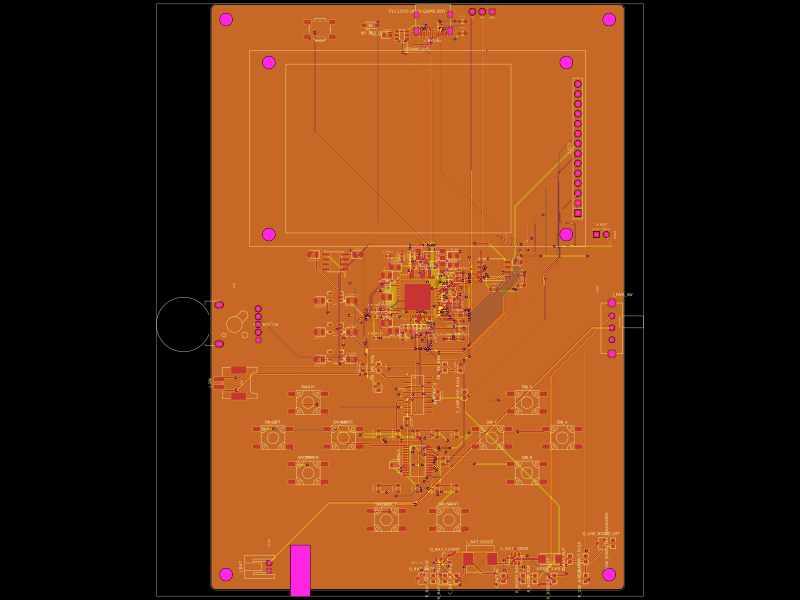
PCB
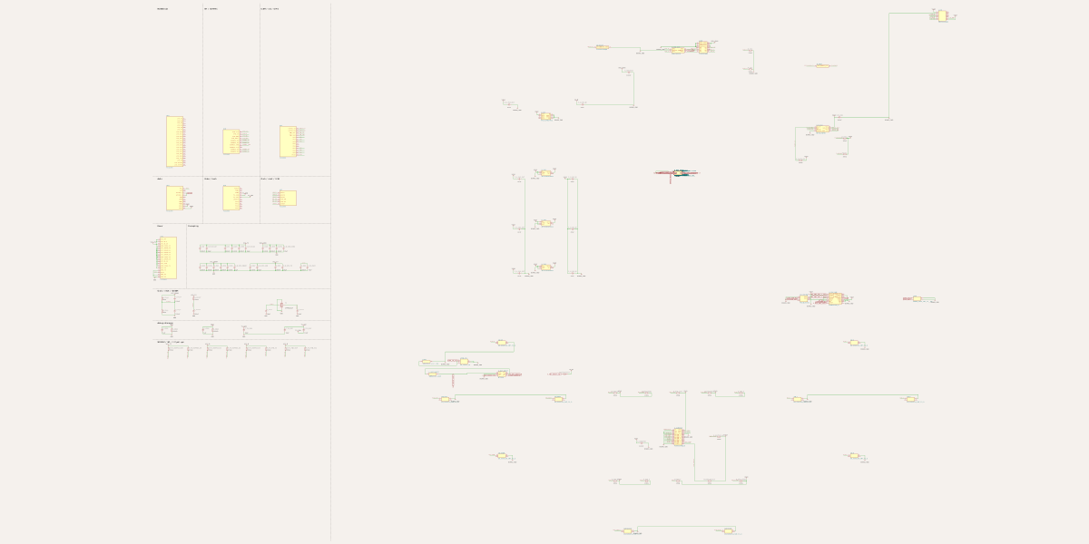
Schematic
import { TYPE_C_31_M_12 } from "./imports/TYPE_C_31_M_12"
import { KH_6X6X15H_SMT_FS_D } from "./imports/KH_6X6X15H_SMT_FS_D"
import { S2B_PH_K_S_LF__SN_ } from "./imports/S2B_PH_K_S_LF__SN_"
import { SK_12E12_G5 } from "./imports/SK_12E12_G5"
import { MT3608 } from "./imports/MT3608"
import { SMMS0630_220M } from "./imports/SMMS0630_220M"
import { SS34 } from "./imports/SS34"
import { B5819W_SL } from "./imports/B5819W_SL"
import { CL10A106KP8NNNC } from "./imports/CL10A106KP8NNNC"
import { CL10A226MQ8NRNC } from "./imports/CL10A226MQ8NRNC"
import { A_0603WAF9532T5E } from "./imports/A_0603WAF9532T5E"
import { FRC0603F1302TS } from "./imports/FRC0603F1302TS"
import { A_0603WAF1003T5E } from "./imports/A_0603WAF1003T5E"
import { AO3401A } from "./imports/AO3401A"
import { MMBT3904_RANGE_100_300_ } from "./imports/MMBT3904_RANGE_100_300_"
import { SM02B_PASS_TBT_LF__SN_ } from "./imports/SM02B_PASS_TBT_LF__SN_"
import { PAM8403DR_H } from "./imports/PAM8403DR_H"
import { BLM18PG121SN1D } from "./imports/BLM18PG121SN1D"
import { RK10J12E002L } from "./imports/RK10J12E002L"
import { PCA9535PW_118 } from "./imports/PCA9535PW_118"
import { PM254_1_14_Z_8_5 } from "./imports/PM254_1_14_Z_8_5"
import { footprints } from "./footprints"
import { routingBoundaryRef } from "./routing-boundary"
import { F1C100SModule } from "./modules/f1c100s/src"
import { AutoroutingPipelineSolver7_MultiGraph } from "@tscircuit/capacity-autorouter"
import boardRoutes from "./imports/board-routes.json"

const USE_PRECOMPUTED_ROUTES = true

const normalizeAutorouterInput = (value: any): any => {
  if (Array.isArray(value)) return value.map(normalizeAutorouterInput)
  if (!value || typeof value !== "object") return value
  const normalized = Object.fromEntries(
    Object.entries(value).map(([key, child]) => [key, normalizeAutorouterInput(child)]),
  ) as Record<string, any>
  if (normalized.layer !== undefined && normalized.layers !== undefined) delete normalized.layer
  return normalized
}

class FabricationAutorouter {
  private solver: any
  private running = false
  private timer: ReturnType<typeof setTimeout> | undefined
  private handlers: Record<"complete" | "error" | "progress", Array<(event: any) => void>> = {
    complete: [], error: [], progress: [],
  }

  constructor(simpleRouteJson: any) {
    const normalizedInput = normalizeAutorouterInput(simpleRouteJson)
    normalizedInput.obstacles.push({
      type: "rect",
      center: { x: 0, y: 0 },
      width: 25.6,
      height: 25.6,
      layers: ["top", "inner1", "inner2", "bottom"],
      connectedTo: [],
    })
    this.solver = USE_PRECOMPUTED_ROUTES && boardRoutes.length > 0
      ? null
      : new AutoroutingPipelineSolver7_MultiGraph(normalizedInput)
  }

  on(event: "complete" | "error" | "progress", handler: (event: any) => void) {
    this.handlers[event].push(handler)
  }

  start() {
    if (this.running) return
    this.running = true
    if (!this.solver) {
      queueMicrotask(() => {
        this.running = false
        for (const handler of this.handlers.complete) {
          handler({ type: "complete", traces: structuredClone(boardRoutes) })
        }
      })
      return
    }
    void this.runBatch()
  }

  private async runBatch() {
    try {
      const started = Date.now()
      while (this.running && !this.solver.solved && !this.solver.failed && Date.now() - started < 200) {
        if (typeof this.solver.stepAsync === "function") await this.solver.stepAsync()
        else this.solver.step()
      }
      if (this.solver.failed) {
        this.running = false
        for (const handler of this.handlers.error) handler({ type: "error", error: new Error(this.solver.error || "Routing failed") })
      } else if (this.solver.solved) {
        this.running = false
        const traces = structuredClone(this.solver.getOutputSimplifiedPcbTraces())
        for (const trace of traces) {
          for (let i = 1; i < trace.route.length; i++) {
            const previous = trace.route[i - 1]
            const current = trace.route[i]
            if (previous.route_type !== "wire" || current.route_type !== "wire" || previous.layer === current.layer) continue
            if (current.end_pcb_port_id) current.layer = previous.layer
            else if (previous.start_pcb_port_id) previous.layer = current.layer
          }
        }
        for (const handler of this.handlers.complete) handler({ type: "complete", traces })
      } else if (this.running) {
        for (const handler of this.handlers.progress) {
          handler({ type: "progress", progress: this.solver.progress, phase: this.solver.getCurrentPhase?.() ?? this.solver.getSolverName?.() })
        }
        this.timer = setTimeout(() => void this.runBatch(), 0)
      }
    } catch (error) {
      this.running = false
      const asError = error instanceof Error ? error : new Error(String(error))
      for (const handler of this.handlers.error) handler({ type: "error", error: asError })
    }
  }

  stop() {
    this.running = false
    if (this.timer) clearTimeout(this.timer)
  }
}

const fabricationAutorouter = async (simpleRouteJson: any) => new FabricationAutorouter(simpleRouteJson)

const connect = (part: string, nets: string[]) => nets.map((net, i) =>
  net ? <trace key={`${part}-${i}`} from={`.${part} > .pin${i + 1}`} to={`net.${net}`} /> : null)

const capacitor = (
  name: string,
  value: string,
  net: string,
  x: number,
  y: number,
  rotation = 0,
  target?: string,
  footprint = "0603",
  manufacturerPartNumber?: string,
  jlcpcb?: string,
) => <>
  <capacitor
    name={name}
    capacitance={value}
    footprint={footprint}
    manufacturerPartNumber={manufacturerPartNumber}
    supplierPartNumbers={jlcpcb ? { jlcpcb: [jlcpcb] } : undefined}
    pcbX={x}
    pcbY={y}
    pcbRotation={rotation}
    schX={x}
    schY={y}
  />
  {/* Power nets are represented as aggregate trees by circuit-json. These limits
      therefore bound the complete rail, not only this capacitor's local branch. */}
  <trace from={`.${name} > .pin1`} to={target ?? `net.${net}`} maxLength={target ? 100 : undefined} />
  <trace from={`.${name} > .pin2`} to="net.BOARD_GND" maxLength={10000} />
</>

const decoupler = (name: string, net: string, x: number, y: number, target?: string) =>
  capacitor(name, "100nF", net, x, y, 0, target, "0603", "CC0603KRX7R9BB104", "C14663")

const resistor = (
  name: string,
  value: string,
  a: string,
  b: string,
  x: number,
  y: number,
  rotation = 0,
  manufacturerPartNumber?: string,
  jlcpcb?: string,
) => <>
  <resistor
    name={name}
    resistance={value}
    footprint="0603"
    manufacturerPartNumber={manufacturerPartNumber}
    supplierPartNumbers={jlcpcb ? { jlcpcb: [jlcpcb] } : undefined}
    pcbX={x}
    pcbY={y}
    pcbRotation={rotation}
    schX={x}
    schY={y}
  />
  {connect(name, [a, b])}
</>

const resistor10k = (name: string, a: string, b: string, x: number, y: number, rotation = 0) =>
  resistor(name, "10k", a, b, x, y, rotation, "FRC0603F1002TS", "C2906982")

const ldoSo8 = (name: string, voltage: string, input: string, output: string, x: number, y: number) => <>
  <chip name={name} manufacturerPartNumber={`AP2112M-${voltage}TRG1`}
    footprint={footprints.so8}
    pinLabels={{pin1:"OUT",pin2:"NC2",pin3:"NC3",pin4:"NC4",pin5:"EN",pin6:"GND6",pin7:"GND7",pin8:"IN"}}
    pcbX={x} pcbY={y} schX={x} schY={y} />
  {connect(name, [output,"","","",input,"BOARD_GND","BOARD_GND",input])}
  {capacitor(`C_${name}_IN`, "4.7uF", input, x+5.8, y+1.905, 0, `.${name} > .pin8`, "0805", "GRM21BR71C475KE51L", "C408144")}
  {capacitor(`C_${name}_OUT`, "4.7uF", output, x-5.8, y+1.905, 180, `.${name} > .pin1`, "0805", "GRM21BR71C475KE51L", "C408144")}
</>

const ldoK = (name: string, voltage: string, output: string, x: number, y: number, mpn = `AP2112K-${voltage}TRG1`) => <>
  <chip name={name} manufacturerPartNumber={mpn}
    footprint="dfn6_missing(5)_p0.95mm_w3.5mm_pw0.5mm_pl0.9mm_pin1location(rightside,bottom)"
    pinLabels={{pin1:"IN",pin2:"GND",pin3:"EN",pin4:"NC",pin5:"OUT"}}
    pinAttributes={{pin2:{requiresGround:true},pin4:{doNotConnect:true}}}
    pcbX={x} pcbY={y} schX={x} schY={y} />
  {connect(name, ["V3V3","BOARD_GND","V3V3","",output])}
  {capacitor(`C_${name}_IN`, "4.7uF", "V3V3", x+4.2, y-0.95, 0, `.${name} > .pin1`, "0805", "GRM21BR71C475KE51L", "C408144")}
  {capacitor(`C_${name}_OUT`, "4.7uF", output, x-4.2, y-0.95, 180, `.${name} > .pin5`, "0805", "GRM21BR71C475KE51L", "C408144")}
</>

const button = (name: string, net: string, x: number, y: number) => <>
  <KH_6X6X15H_SMT_FS_D name={name} pcbX={x} pcbY={y} schX={x} schY={y} />
  <trace from={`.${name} > .pin1`} to={`net.${net}`} />
  <trace from={`.${name} > .pin4`} to="net.BOARD_GND" />
</>

const displayPinLabels = {
  pin1: "VCC",
  pin2: "GND",
  pin3: "CS",
  pin4: "RESET",
  pin5: "DC_RS",
  pin6: "SDI_MOSI",
  pin7: "SCK",
  pin8: "LED",
  pin9: "SDO_MISO",
  pin10: "T_CLK",
  pin11: "T_CS",
  pin12: "T_DIN",
  pin13: "T_DO",
  pin14: "T_IRQ",
} as const

const buttonNets = [
  "BTN_UP", "BTN_DOWN", "BTN_LEFT", "BTN_RIGHT", "BTN_A",
  "BTN_B", "BTN_X", "BTN_Y", "BTN_SELECT", "BTN_START",
] as const

export default () => <board
  title="F1C100S Linux Game Boy handheld"
  width={106}
  height={150}
  borderRadius={1.5}
  layers={4}
  minTraceWidth={0.12}
  minViaPadDiameter={0.45}
  minViaHoleDiameter={0.3}
  autorouter={{ algorithmFn: fabricationAutorouter }}
  {...{ref:routingBoundaryRef}}
  schLayout={{layoutMode:"relative"}}
  schTraceAutoLabelEnabled
  schMaxTraceDistance={3}
>
  <autoroutingphase autorouter={{ algorithmFn: fabricationAutorouter }} minTraceToPadEdgeClearance={0.13} minPadEdgeToPadEdgeClearance={0.13} minViaEdgeToPadEdgeClearance={0.13} />
  <keepout shape="rect" width={25.6} height={25.6} pcbX={0} pcbY={0}
    layers={["top","inner1","inner2","bottom"]} excludeRefs={[".SOC *"]} />
  <keepout shape="rect" width={0.8} height={1.1} pcbX={13.3} pcbY={2.65}
    layers={["top","inner1","inner2","bottom"]} excludeRefs={[".SOC *"]} />

  <net name="BOARD_GND" isGroundNet />
  <net name="USB_VBUS" isPowerNet nominalTraceWidth={0.4} />
  <net name="V5_IN" isPowerNet nominalTraceWidth={0.4} />
  <net name="V3V3" isPowerNet nominalTraceWidth={0.2} />
  <net name="V2V8" isPowerNet />
  <net name="V2V5" isPowerNet />
  <net name="V1V2" isPowerNet />

  <F1C100SModule name="SOC" layoutProfile="native" pcbX={0} pcbY={0} schX={-70} schY={0}
    connections={{
      GND:"net.BOARD_GND", VDD_CORE:"net.V1V2", VCC_DRAM:"net.V2V5",
      VCC_IO:"net.V3V3", VCC_USB:"net.V3V3", AVCC:"net.V2V8",
      VCC_HP:"net.V3V3", VCC_TV:"net.V3V3",
      SPI0_CLK:"net.FLASH_CLK", SPI0_CS:"net.SOC_FLASH_CS",
      SPI0_MOSI:"net.FLASH_MOSI", SPI0_MISO:"net.FLASH_MISO",
      PE7:"net.LCD_CS", PE8:"net.LCD_MOSI", PE9:"net.LCD_SCK", PE10:"net.LCD_MISO",
      TWI0_SDA:"net.I2C_SDA", TWI0_SCL:"net.I2C_SCL",
      UART0_TX:"net.UART_TX", UART0_RX:"net.UART_RX",
      USB_DM:"net.USB_N", USB_DP:"net.USB_P", RESET:"net.RESET_N",
      PE2:"net.LCD_DC", PE3:"net.LCD_RESET", PE4:"net.GAMEPAD_INT",
      HPL:"net.CODEC_HPL",
    }} />

  {/* Four-rail Linux compute power tree. */}
  {ldoSo8("U_3V3", "3.3", "V5_IN", "V3V3", -21, 9)}
  {ldoK("U_2V5", "2.5", "V2V5", -21, 0)}
  {ldoK("U_1V2", "1.2", "V1V2", -21, -8)}
  {ldoK("U_2V8", "2.8", "V2V8", -21, -15, "AP2127K-2.8TRG1")}

  {/* 16 MiB SPI0 boot flash with removable chip-select shunt for USB FEL recovery. */}
  <chip name="U_FLASH" manufacturerPartNumber="W25Q128JVSIQ"
    footprint={footprints.flash}
    pinLabels={{pin1:"CS_N",pin2:"DO",pin3:"WP_N",pin4:"BOARD_GND",pin5:"DI",pin6:"CLK",pin7:"HOLD_N",pin8:"VCC"}}
    pcbX={19.5} pcbY={7} schX={23} schY={7} />
  {connect("U_FLASH", ["FLASH_CS","FLASH_MISO","FLASH_WP","BOARD_GND","FLASH_MOSI","FLASH_CLK","FLASH_HOLD","V3V3"])}
  {decoupler("C_FLASH", "V3V3", 25.7, 8.905, ".U_FLASH > .pin8")}
  {resistor10k("R_WP", "FLASH_WP", "V3V3", 26.5, 3)}
  {resistor10k("R_HOLD", "FLASH_HOLD", "V3V3", 26.5, 5.5)}
  {resistor10k("R_FLASH_CS", "FLASH_CS", "V3V3", 19.5, 2)}
  <chip name="JP_BOOT" footprint="pinrow2_p2.54" pinLabels={{pin1:"SOC_CS",pin2:"FLASH_CS"}}
    pcbX={47} pcbY={16} schX={23} schY={17} />
  {connect("JP_BOOT", ["SOC_FLASH_CS","FLASH_CS"])}

  {/* USB-C data/programming at the top edge; Schottky OR isolates battery power. */}
  <group name="USB_ASSEMBLY" pcbX={0} pcbY={51}>
    <TYPE_C_31_M_12 name="J_USB" pcbX={4} pcbY={18.5} pcbRotation={180} schX={4} schY={20} />
    {connect("J_USB", ["BOARD_GND","BOARD_GND","BOARD_GND","BOARD_GND","","USB_CC1","USB_N","USB_P","","","","USB_CC2","BOARD_GND","BOARD_GND","USB_VBUS","USB_VBUS"])}
    <trace name="USB_DM_REVERSIBLE" from=".J_USB > .pin7" to=".J_USB > .pin9" maxLength={20}
      pcbPath={[".J_USB > .pin7",{x:-0.750062,y:3.1},{x:0.249936,y:3.1},".J_USB > .pin9"]} />
    <trace name="USB_DP_REVERSIBLE" from=".J_USB > .pin8" to=".J_USB > .pin10" maxLength={20}
      pcbPath={[".J_USB > .pin8",{x:-0.249936,y:1.25},{x:0.750062,y:1.25},".J_USB > .pin10"]} />
    {resistor("R_CC1", "5.1k", "USB_CC1", "BOARD_GND", 11.5, 19.5, 0, "0603WAF5101T5E", "C23186")}
    {resistor("R_CC2", "5.1k", "USB_CC2", "BOARD_GND", 11.5, 16.5, 0, "0603WAF5101T5E", "C23186")}
    <chip name="U_USB_ESD" manufacturerPartNumber="USBLC6-2SC6" footprint="sot23_6"
      pinLabels={{pin1:"DM1",pin2:"BOARD_GND",pin3:"DP1",pin4:"DP2",pin5:"VBUS",pin6:"DM2"}}
      pcbX={-4} pcbY={16} pcbRotation={180} schX={0} schY={19.5} />
    {connect("U_USB_ESD", ["USB_N","BOARD_GND","USB_P","USB_P","USB_VBUS","USB_N"])}
    {decoupler("C_USB_ESD", "USB_VBUS", -7.8, 16, ".U_USB_ESD > .pin5")}
    <B5819W_SL name="D_USB_OR" pcbX={-12} pcbY={18.5} pcbRotation={180} />
    <trace from=".D_USB_OR > .anode" to="net.USB_VBUS" thickness={0.4} />
    <trace from=".D_USB_OR > .cathode" to="net.V5_IN" thickness={0.4} />
    {(["TX","RX","GND"] as const).map((signal,i)=><group key={signal} pcbX={0} pcbY={0}>
      <testpoint name={`TP_UART_${signal}`} pcbX={14+i*2.54} pcbY={22}
        footprint={<footprint><platedhole portHints={["pin1"]} holeDiameter={1} outerDiameter={1.8} shape="circle" /></footprint>} />
      <trace from={`.TP_UART_${signal} > .pin1`} to={`net.${signal==="GND"?"BOARD_GND":`UART_${signal}`}`} />
      <silkscreentext text={signal} pcbX={14+i*2.54} pcbY={20.5} fontSize={0.65} />
    </group>)}
  </group>

  <chip name="SW_RESET" footprint={footprints.reset} manufacturerPartNumber="TL3342F160QG"
    pinLabels={{pin1:"RESET",pin2:"BOARD_GND"}} pcbX={-25} pcbY={68.5} schX={-12} schY={20} />
  {connect("SW_RESET", ["RESET_N","BOARD_GND"])}

  {/* LCDWiki MSP2807 / ILI9341 removable SPI display connector and mechanics. */}
  <PM254_1_14_Z_8_5 name="J_LCD"
    pcbX={41} pcbY={38} pcbRotation={90} schX={42} schY={25} />
  {connect("J_LCD", ["V5_IN","BOARD_GND","LCD_CS","LCD_RESET","LCD_DC","LCD_MOSI","LCD_SCK","V3V3","LCD_MISO","","","","",""])}
  <silkscreenrect pcbX={0} pcbY={38} width={86} height={50} />
  <silkscreenrect pcbX={-4.9} pcbY={38} width={57.6} height={43.2} />
  {([-38.04,38.04] as const).flatMap(x => ([16,60] as const).map(y =>
    <hole name={`LCD_MH_${x}_${y}`} diameter={3.2} pcbX={x} pcbY={y} />))}

  {/* PCA9535 game-control input bank, address 0x20, with interrupt to PE4. */}
  <PCA9535PW_118 name="U_GAMEPAD" pcbX={0} pcbY={-42} pcbRotation={90} schX={0} schY={-42} />
  {connect("U_GAMEPAD", [
    "GAMEPAD_INT","BOARD_GND","BOARD_GND",
    "BTN_UP","BTN_DOWN","BTN_LEFT","BTN_RIGHT","BTN_A","BTN_B","BTN_X","BTN_Y",
    "BOARD_GND","BTN_SELECT","BTN_START","","","","","","","BOARD_GND","I2C_SCL","I2C_SDA","V3V3",
  ])}
  {decoupler("C_GAMEPAD", "V3V3", -5.8, -43, ".U_GAMEPAD > .pin24")}
  {resistor10k("R_GAMEPAD_INT", "GAMEPAD_INT", "V3V3", 6.5, -42, 90)}
  {buttonNets.map((net, i) => resistor10k(`R_${net}`, net, "V3V3", -10 + (i % 5) * 5, i < 5 ? -35 : -49, 90))}

  {button("SW_UP", "BTN_UP", -28, -27)}
  {button("SW_DOWN", "BTN_DOWN", -28, -45)}
  {button("SW_LEFT", "BTN_LEFT", -37, -36)}
  {button("SW_RIGHT", "BTN_RIGHT", -19, -36)}
  {button("SW_A", "BTN_A", 37, -36)}
  {button("SW_B", "BTN_B", 28, -45)}
  {button("SW_X", "BTN_X", 28, -27)}
  {button("SW_Y", "BTN_Y", 19, -36)}
  {button("SW_SELECT", "BTN_SELECT", -8, -57)}
  {button("SW_START", "BTN_START", 8, -57)}

  {/* Native F1C100S codec left output into a filtered mono speaker amplifier. */}
  <PAM8403DR_H name="U_SPK_AMP" pcbX={0} pcbY={-25} pcbRotation={-90} schX={25} schY={-20} />
  <RK10J12E002L name="RV_VOLUME" pcbX={-45.4} pcbY={-7} pcbRotation={90} schX={20} schY={-20} />
  <SM02B_PASS_TBT_LF__SN_ name="J_SPK" pcbX={-48} pcbY={-22} pcbRotation={90} schX={38} schY={-20} />
  <capacitor name="C_AUDIO_COUPLE" capacitance="1uF" footprint="0603"
    manufacturerPartNumber="CL10B105KA8NNNC" supplierPartNumbers={{jlcpcb:["C29936"]}}
    pcbX={-10} pcbY={-23} pcbRotation={90} />
  <capacitor name="C_AMP_VDD" capacitance="1uF" footprint="0603"
    manufacturerPartNumber="CL10B105KA8NNNC" supplierPartNumbers={{jlcpcb:["C29936"]}}
    pcbX={5} pcbY={-25} pcbRotation={90} />
  <CL10A226MQ8NRNC name="C_AMP_VDD_BULK" pcbX={12} pcbY={-25} pcbRotation={90} />
  <capacitor name="C_AMP_VREF" capacitance="1uF" footprint="0603"
    manufacturerPartNumber="CL10B105KA8NNNC" supplierPartNumbers={{jlcpcb:["C29936"]}}
    pcbX={-2.7356} pcbY={-32} pcbRotation={270} />
  <BLM18PG121SN1D name="FB_SPK_POS" pcbX={-10} pcbY={-18} pcbRotation={90} />
  <BLM18PG121SN1D name="FB_SPK_NEG" pcbX={7} pcbY={-18} pcbRotation={90} />
  <capacitor name="C_SPK_EMI_POS" capacitance="220pF" footprint="0603"
    manufacturerPartNumber="CC0603JRNPO9BN221" supplierPartNumbers={{jlcpcb:["C106210"]}}
    pcbX={-14} pcbY={-18} pcbRotation={90} />
  <capacitor name="C_SPK_EMI_NEG" capacitance="220pF" footprint="0603"
    manufacturerPartNumber="CC0603JRNPO9BN221" supplierPartNumbers={{jlcpcb:["C106210"]}}
    pcbX={11} pcbY={-18} pcbRotation={90} />
  <trace from="net.CODEC_HPL" to=".C_AUDIO_COUPLE > .pin1" />
  <trace from=".C_AUDIO_COUPLE > .pin2" to=".RV_VOLUME > .pin3" />
  <trace from=".RV_VOLUME > .pin2" to=".U_SPK_AMP > .INL" />
  <trace from=".RV_VOLUME > .pin1" to="net.BOARD_GND" />
  <trace from=".U_SPK_AMP > .INR" to="net.BOARD_GND" />
  <trace from=".U_SPK_AMP > .MUTE" to="net.V3V3" />
  <trace from=".U_SPK_AMP > .SHND" to="net.V3V3" />
  <trace from=".U_SPK_AMP > .VDD" to="net.V5_IN" thickness={0.4} />
  <trace from=".U_SPK_AMP > .PVDD1" to="net.V5_IN" thickness={0.4} />
  <trace from=".U_SPK_AMP > .PVDD2" to="net.V5_IN" thickness={0.4} />
  <trace from=".U_SPK_AMP > .GND" to="net.BOARD_GND" />
  <trace from=".U_SPK_AMP > .PGND1" to="net.BOARD_GND" thickness={0.25} />
  <trace from=".U_SPK_AMP > .PGND2" to="net.BOARD_GND" thickness={0.25} />
  <trace from=".C_AMP_VDD > .pin1" to="net.V5_IN" thickness={0.4} />
  <trace from=".C_AMP_VDD > .pin2" to="net.BOARD_GND" />
  <trace from=".C_AMP_VDD_BULK > .pin1" to="net.V5_IN" thickness={0.4} />
  <trace from=".C_AMP_VDD_BULK > .pin2" to="net.BOARD_GND" />
  <trace from=".U_SPK_AMP > .VREF" to=".C_AMP_VREF > .pin1" maxLength={5} />
  <trace from=".C_AMP_VREF > .pin2" to="net.BOARD_GND" maxLength={10000} />
  <trace from=".U_SPK_AMP > .OUT_L_POS" to=".FB_SPK_POS > .pin1" thickness={0.25} />
  <trace from=".FB_SPK_POS > .pin2" to=".J_SPK > .pin1" thickness={0.25} />
  <trace from=".FB_SPK_POS > .pin2" to=".C_SPK_EMI_POS > .pin1" />
  <trace from=".C_SPK_EMI_POS > .pin2" to="net.BOARD_GND" />
  <trace from=".U_SPK_AMP > .OUT_L_NEG" to=".FB_SPK_NEG > .pin1" thickness={0.25} />
  <trace from=".FB_SPK_NEG > .pin2" to=".J_SPK > .pin2" thickness={0.25} />
  <trace from=".FB_SPK_NEG > .pin2" to=".C_SPK_EMI_NEG > .pin1" />
  <trace from=".C_SPK_EMI_NEG > .pin2" to="net.BOARD_GND" />
  <trace from=".J_SPK > .pin3" to="net.BOARD_GND" />
  <trace from=".J_SPK > .pin4" to="net.BOARD_GND" />

  {/* 3xAA battery boost. USB presence disconnects and disables the battery path. */}
  <S2B_PH_K_S_LF__SN_ name="J_BAT" pcbX={-38} pcbY={-69} pcbRotation={90} schX={-40} schY={-30} />
  {/* Unplated edge-open notch: extends 1.5 mm beyond the lower board edge. */}
  <cutout name="BAT_CABLE_NOTCH" shape="rect" width="5mm" height="13mm"
    pcbX="-30mm" pcbY="-70mm" />
  <SK_12E12_G5 name="J_PWR_SW" pcbX={49.7} pcbY={-8} schX={-34} schY={-30} />
  <MT3608 name="U_BAT_BOOST" pcbX={25} pcbY={-67} schX={-28} schY={-32} />
  <SMMS0630_220M name="L_BAT_BOOST" pcbX={16} pcbY={-67} schX={-39} schY={-32} />
  <SS34 name="D_BAT_BOOST" pcbX={34} pcbY={-67} pcbRotation={180} schX={-18} schY={-32} />
  <CL10A106KP8NNNC name="C_BAT_IN" pcbX={22} pcbY={-72} pcbRotation={90} />
  <CL10A226MQ8NRNC name="C_BAT_OUT" pcbX={39} pcbY={-67} pcbRotation={90} />
  <CL10A106KP8NNNC name="C_BAT_IN_BULK" pcbX={10} pcbY={-72} pcbRotation={90} />
  <CL10A226MQ8NRNC name="C_BAT_OUT_BULK" pcbX={43} pcbY={-67} pcbRotation={90} />
  <A_0603WAF9532T5E name="R_BOOST_TOP" pcbX={30} pcbY={-72} pcbRotation={90} />
  <FRC0603F1302TS name="R_BOOST_BOT" pcbX={27} pcbY={-72} pcbRotation={90} />
  <A_0603WAF1003T5E name="R_BOOST_EN_PULLUP" pcbX={35} pcbY={-72} pcbRotation={90} />
  <A_0603WAF1003T5E name="R_USB_BOOST_OFF" pcbX={43} pcbY={-72} pcbRotation={90} />
  <A_0603WAF1003T5E name="R_USB_BOOST_OFF_PULLDOWN" pcbX={50} pcbY={-63} pcbRotation={90} />
  <AO3401A name="Q_BAT_CUTOFF" pcbX={7} pcbY={-67} />
  <A_0603WAF1003T5E name="R_BAT_GATE_PULLUP" pcbX={7} pcbY={-72} pcbRotation={90} />
  <A_0603WAF1003T5E name="R_BAT_GATE_BASE" pcbX={4} pcbY={-72} pcbRotation={90} />
  <MMBT3904_RANGE_100_300_ name="Q_BAT_GATE" pcbX={1} pcbY={-72} />
  <MMBT3904_RANGE_100_300_ name="Q_USB_BOOST_OFF" pcbX={47} pcbY={-63} />
  <trace from=".J_BAT > .pin1" to=".J_PWR_SW > .pin2" thickness={0.4} />
  <trace from=".J_BAT > .pin2" to="net.BOARD_GND" thickness={0.4} />
  <trace from=".J_PWR_SW > .pin1" to=".Q_BAT_CUTOFF > .S" thickness={0.4} />
  <trace from=".J_PWR_SW > .pin4" to="net.BOARD_GND" />
  <trace from=".J_PWR_SW > .pin5" to="net.BOARD_GND" />
  <trace from=".J_PWR_SW > .pin1" to=".R_BOOST_EN_PULLUP > .pin1" />
  <trace from=".R_BOOST_EN_PULLUP > .pin2" to=".U_BAT_BOOST > .EN" />
  <trace from=".Q_USB_BOOST_OFF > .C" to=".U_BAT_BOOST > .EN" />
  <trace from=".Q_USB_BOOST_OFF > .E" to="net.BOARD_GND" />
  <trace from="net.USB_VBUS" to=".R_USB_BOOST_OFF > .pin1" />
  <trace from=".R_USB_BOOST_OFF > .pin2" to=".Q_USB_BOOST_OFF > .B" />
  <trace from=".Q_USB_BOOST_OFF > .B" to=".R_USB_BOOST_OFF_PULLDOWN > .pin1" />
  <trace from=".R_USB_BOOST_OFF_PULLDOWN > .pin2" to="net.BOARD_GND" />
  <trace from=".Q_BAT_CUTOFF > .D" to=".U_BAT_BOOST > .IN" thickness={0.4} />
  <trace from=".J_PWR_SW > .pin1" to=".R_BAT_GATE_PULLUP > .pin1" />
  <trace from=".R_BAT_GATE_PULLUP > .pin2" to=".Q_BAT_CUTOFF > .G" />
  <trace from=".Q_BAT_GATE > .C" to=".Q_BAT_CUTOFF > .G" />
  <trace from=".Q_BAT_GATE > .E" to="net.BOARD_GND" />
  <trace from=".U_BAT_BOOST > .EN" to=".R_BAT_GATE_BASE > .pin1" />
  <trace from=".R_BAT_GATE_BASE > .pin2" to=".Q_BAT_GATE > .B" />
  <trace from=".Q_BAT_CUTOFF > .D" to=".L_BAT_BOOST > .pin1" thickness={0.4} />
  <trace from=".L_BAT_BOOST > .pin2" to=".U_BAT_BOOST > .SW" thickness={0.4} />
  <trace from=".U_BAT_BOOST > .SW" to=".D_BAT_BOOST > .anode" thickness={0.4} />
  <trace from=".D_BAT_BOOST > .cathode" to="net.V5_IN" thickness={0.4} />
  <trace from=".U_BAT_BOOST > .GND" to="net.BOARD_GND" thickness={0.4} />
  <trace from=".C_BAT_IN > .pin1" to=".Q_BAT_CUTOFF > .D" thickness={0.4} />
  <trace from=".C_BAT_IN > .pin2" to="net.BOARD_GND" thickness={0.4} />
  <trace from=".C_BAT_IN_BULK > .pin1" to=".Q_BAT_CUTOFF > .D" thickness={0.4} />
  <trace from=".C_BAT_IN_BULK > .pin2" to="net.BOARD_GND" thickness={0.4} />
  <trace from=".C_BAT_OUT > .pin1" to=".D_BAT_BOOST > .cathode" thickness={0.4} />
  <trace from=".C_BAT_OUT > .pin2" to="net.BOARD_GND" thickness={0.4} />
  <trace from=".C_BAT_OUT_BULK > .pin1" to=".D_BAT_BOOST > .cathode" thickness={0.4} />
  <trace from=".C_BAT_OUT_BULK > .pin2" to="net.BOARD_GND" thickness={0.4} />
  <trace from=".D_BAT_BOOST > .cathode" to=".R_BOOST_TOP > .pin1" />
  <trace from=".R_BOOST_TOP > .pin2" to=".U_BAT_BOOST > .FB" />
  <trace from=".U_BAT_BOOST > .FB" to=".R_BOOST_BOT > .pin1" />
  <trace from=".R_BOOST_BOT > .pin2" to="net.BOARD_GND" />

  {/* Chassis mechanics and front-panel labeling. */}
  {([-49,49] as const).flatMap(x => ([-71,71] as const).map(y =>
    <hole name={`MH_${x}_${y}`} diameter={3.2} pcbX={x} pcbY={y} />))}
  <silkscreentext text="F1C100S LINUX GAME BOY" pcbX={0} pcbY={73} fontSize={1.1} />
  <silkscreentext text="LCDWIKI 2.8 SPI" pcbX={0} pcbY={63.5} fontSize={0.9} />
  <silkscreentext text="USB-C / FEL" pcbX={4} pcbY={65.5} fontSize={0.75} />
  <silkscreentext text="RESET" pcbX={-25} pcbY={65.5} fontSize={0.7} />
  <silkscreentext text="UP" pcbX={-28} pcbY={-23} fontSize={0.8} />
  <silkscreentext text="DOWN" pcbX={-28} pcbY={-41} fontSize={0.8} />
  <silkscreentext text="LEFT" pcbX={-37} pcbY={-32} fontSize={0.8} />
  <silkscreentext text="RIGHT" pcbX={-19} pcbY={-32} fontSize={0.8} />
  <silkscreentext text="A" pcbX={37} pcbY={-32} fontSize={0.9} />
  <silkscreentext text="B" pcbX={28} pcbY={-41} fontSize={0.9} />
  <silkscreentext text="X" pcbX={28} pcbY={-23} fontSize={0.9} />
  <silkscreentext text="Y" pcbX={19} pcbY={-32} fontSize={0.9} />
  <silkscreentext text="SELECT" pcbX={-8} pcbY={-53} fontSize={0.7} />
  <silkscreentext text="START" pcbX={8} pcbY={-53} fontSize={0.7} />
  <silkscreentext text="3xAA" pcbX={-38} pcbY={-63} fontSize={0.7} pcbRotation={90} />
  <silkscreentext text="VOL" pcbX={-47} pcbY={3} fontSize={0.7} pcbRotation={90} />
  <silkscreentext text="PWR" pcbX={46} pcbY={2} fontSize={0.7} pcbRotation={90} />
  <silkscreentext text="SPK" pcbX={-45} pcbY={-22} fontSize={0.7} pcbRotation={90} />
  <silkscreentext text="BOOT" pcbX={50.5} pcbY={16} fontSize={0.7} pcbRotation={90} />
  <silkscreentext text="REV 1.0" pcbX={0} pcbY={-68} fontSize={0.65} />

  {(["top","inner1","inner2","bottom"] as const).map(layer =>
    <copperpour layer={layer} connectsTo="net.BOARD_GND" clearance={0.15}
      boardEdgeMargin={0.3} useThermalReliefs coveredWithSolderMask />)}
</board>