ShiboSoftwareDev/clip-on-battery-meter-2
The code defines virtual representations of various electronic components—such as a BAT54WS Schottky diode and LM339 and LM393 voltage comparators—with physical pin configurations, footprints, and 3D models for PCB design.
- Version
- 1.0.13
- License
- unset
- Stars
- 0
imports/MY_18650_02.tsx
import type { ConnectorProps } from "@tscircuit/props"

const pinLabels = {
  // Imported from JLC/LCSC part C2979182, MY-18650-02.
  // The manufacturer drawing identifies this part as one 18650 battery terminal,
  // not a complete two-terminal battery holder. All copper belongs to one node.
  // Temporary routing workaround: expose each copper feature as a separate pin
  // so current core does not warn about far-apart pads sharing one port hint.
  pin1: ["pin1"], // right SMT pad
  pin2: ["pin2"], // left SMT pad
  pin3: ["pin3"], // left plated hole
  pin4: ["pin4"], // right plated hole
} as const

const pinAttributes = {
  pin1: { mustBeConnected: true, includeInBoardPinout: true },
  pin2: { mustBeConnected: true, includeInBoardPinout: true },
  pin3: { mustBeConnected: true, includeInBoardPinout: true },
  pin4: { mustBeConnected: true, includeInBoardPinout: true },
} as any

export const MY_18650_02 = (props: ConnectorProps) => {
  return (
    <connector
      pinLabels={pinLabels}
      pinAttributes={pinAttributes}
      supplierPartNumbers={{
  "jlcpcb": [
    "C2979182"
  ]
}}
      manufacturerPartNumber="MY_18650_02"
      footprint={<footprint>
        <smtpad portHints={["pin1"]} pcbX="8.499983mm" pcbY="0mm" width="4.99999mm" height="5.499989mm" shape="rect" />
<smtpad portHints={["pin2"]} pcbX="-8.499983mm" pcbY="0mm" width="4.99999mm" height="3.499993mm" shape="rect" />
<platedhole portHints={["pin3"]} pcbX="-8.000111mm" pcbY="0mm" outerDiameter="1.8499836mm" holeDiameter="0.9249918mm" shape="circle" />
<platedhole portHints={["pin4"]} pcbX="7.999857mm" pcbY="0mm" outerDiameter="1.8499836mm" holeDiameter="0.9249918mm" shape="circle" />
<silkscreenpath route={[{"x":-3.429990599999769,"y":5.619978599999968},{"x":-3.429990599999769,"y":-5.782513199999926}]} />
<silkscreenpath route={[{"x":-3.429990599999769,"y":-5.669991199999913},{"x":6.099987800000235,"y":-5.669991199999913}]} />
<silkscreenpath route={[{"x":-3.429990599999769,"y":5.619978599999968},{"x":6.099987800000235,"y":5.619978599999968}]} />
<silkscreenpath route={[{"x":-5.899988199999825,"y":1.9580351999999266},{"x":-5.899988199999825,"y":5.619978599999968},{"x":-3.429990599999769,"y":5.619978599999968},{"x":-3.429990599999769,"y":8.249970800000028},{"x":6.099987800000235,"y":8.249970800000028}]} />
<silkscreenpath route={[{"x":6.099987800000235,"y":-8.249996200000055},{"x":-3.429990599999769,"y":-8.249996200000055},{"x":-3.429990599999769,"y":-5.669991199999913},{"x":-5.899988199999825,"y":-5.669991199999913},{"x":-5.899988199999825,"y":-1.9580605999999534}]} />
<silkscreenpath route={[{"x":6.099987800000235,"y":-2.9811217999999826},{"x":6.099987800000235,"y":-8.249996200000055}]} />
<silkscreenpath route={[{"x":6.099987800000235,"y":8.249970800000028},{"x":6.099987800000235,"y":2.9811217999999826}]} />
<courtyardoutline outline={[{"x":-11.247310999999968,"y":8.504999999999995},{"x":11.24908900000014,"y":8.504999999999995},{"x":11.24908900000014,"y":-8.504999999999882},{"x":-11.247310999999968,"y":-8.504999999999882},{"x":-11.247310999999968,"y":8.504999999999995}]} />
      </footprint>}
      cadModel={{
        objUrl: "https://modelcdn.tscircuit.com/easyeda_models/assets/C2979182.obj?uuid=17bab5f954174916a1c2399c3b756d35",
        stepUrl: "https://modelcdn.tscircuit.com/easyeda_models/assets/C2979182.step?uuid=17bab5f954174916a1c2399c3b756d35",
        pcbRotationOffset: 0,
        modelOriginPosition: { x: 0, y: 0, z: -0.35000200000000015 },
      }}
      {...props}
    />
  )
}
Related Packages
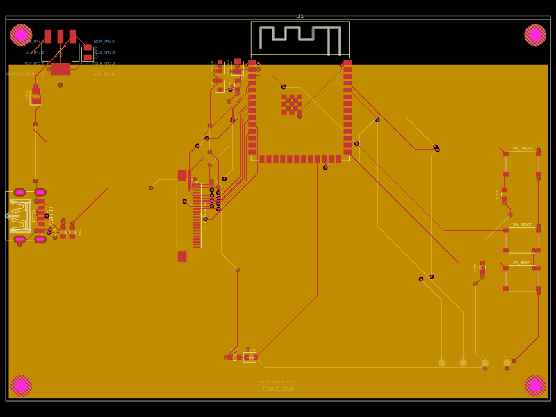 More from this authorShiboSoftwareDev/muse-reterminal-e1001-replacementA four-layer ESP32-S3 e-paper carrier board with USB-C power, AMS1117 3.3V regulation, 24-pin FFC interface, reset/boot and user buttons, status LED, decoupling passives, test points, mounting holes, and ground/power planes.
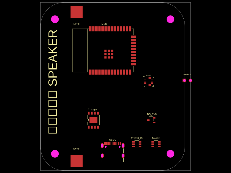 Similar packagemohan-bee/speakerThis code defines configurable 3D models and PCB footprints for various electronic components, including a battery charger IC, a dual Hall sensor, a dual power switch, and a voltage regulator, with detailed pinouts, footprints, and CAD models for schematic and physical design.
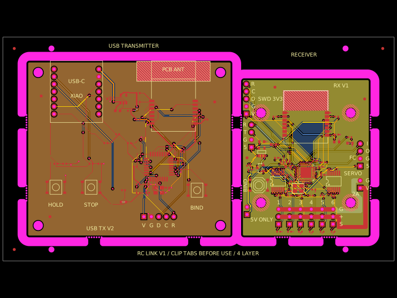 Discover something newmohan-bee/rc-link-breakaway-panelA four-layer RC link panel combining an STM32/E28 2.4‑GHz transmitter with USB-RP2040 socket and an STM32/E28 receiver providing six buffered PWM servo outputs, regulated 3.3‑V power, headers, controls, and protection/decoupling.