ShiboSoftwareDev/cc2340r5-reference-design
A CC2340R5 wireless MCU reference board integrating a 2.4 GHz RF matching network and antenna, 48 MHz/optional 32.768 kHz crystals, DC/DC inductors, decoupling capacitors, reset circuitry, power input, and SWD debug connector.
- Version
- 1.4.0
- License
- unset
- Stars
- 0
index.circuit.tsx
PCB
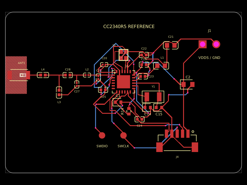
Schematic

import { Fragment } from "react"
import { routeRemaining } from "./routing"
import { propsJsonSchema } from "./props-schema"
import { createPropsParser } from "./scripts/shared/props-parser"
import type { FromSchema } from "json-schema-to-ts"
export { propsJsonSchema } from "./props-schema"
import type { SchematicTextProps } from "@tscircuit/props"
import { CC2340R52E0RGER } from "./imports/cc2340r52e0rger"
import { ABM11W_48_0000MHZ_8_D1X_T3 } from "./imports/abm11w-48-0000mhz-8-d1x-t3"
import { ABS07_32_768KHZ_7_T } from "./imports/abs07-32-768khz-7-t"
import { BM05B_SRSS_TB_LF__SN_ } from "./imports/bm05b-srss-tb-lf-sn"
import { A_2450AT18A100E } from "./imports/a-2450at18a100e"
import { CL05B104KO5NNNC } from "./imports/cl05b104ko5nnnc"
import { GRM033R61A104KE15D } from "./imports/grm033r61a104ke15d"
import { GRM188Z71A106KA73D } from "./imports/grm188z71a106ka73d"
import { CL05A105KA5NQNC } from "./imports/cl05a105ka5nqnc"
import { GJM0335C1H1R5BB01D } from "./imports/gjm0335c1h1r5bb01d"
import { GJM1555C1H1R0BB01D } from "./imports/gjm1555c1h1r0bb01d"
import { LQM18DN100M70L } from "./imports/lqm18dn100m70l"
import { LQP03TN2N8B02D } from "./imports/lqp03tn2n8b02d"
import { LQG15HS2N7S02D } from "./imports/lqg15hs2n7s02d"
import { LQG15HS3N9S02D } from "./imports/lqg15hs3n9s02d"
// Assign every note to the same sheet while retaining the published text prop types.
const Note = (props: SchematicTextProps) => (
<schematictext {...{ ...props, schSheetName: "reference" }} />
)
const sectionMembers: Record<string, string[]> = {
mcu: ["U1"],
power_input: ["J1"],
vdds: ["C1", "C2", "C19", "C20"],
vddr: ["L1", "C21", "C22", "C25"],
vddd: ["C23"],
rf: ["C26", "C27", "C28", "L2", "L3", "L4", "ANT1"],
hf: ["Y2"],
lf: ["Y1", "C14", "C15"],
reset: ["R14", "C24"],
debug: ["J4", "TP1", "TP2"],
}
const schematic = Object.fromEntries(
Object.entries(sectionMembers).flatMap(([section, names]) =>
names.map((name) => [
name,
{ schSheetName: "reference", schSectionName: section },
]),
),
)
export const propsSchema = createPropsParser<FromSchema<typeof propsJsonSchema>>(propsJsonSchema)
export const referenceProps = propsSchema
// The component identities, physical pin mapping, passive values and RF topology
// are extracted from imrishabh18/pedometer 1.1.8, release da16de72-54f3-4684-8f54-a0bf42f941e7.
// Coordinates are redrawn for this standalone MCU reference; the PMIC, gauge,
// accelerometer, USB and display circuits are deliberately outside this package.
export default function Cc2340Reference(
input: Partial<FromSchema<typeof propsJsonSchema>> = {},
) {
const {
externalLfCrystal,
debugHeader,
supplyVoltage,
inputBulkCapacitance,
resetPullupResistance,
} = referenceProps.parse(input)
const supplyLabel = `${supplyVoltage.toFixed(1)}V`
const nets: Record<string, string[]> = {
VDDS: [
"J1.1",
"U1.11",
"U1.18",
"U1.24",
"C1.1",
"C2.1",
"C19.1",
"C20.1",
"R14.1",
],
GND: [
"J1.2",
"U1.23",
"U1.25",
"Y2.2",
"Y2.4",
"C1.2",
"C2.2",
"C19.2",
"C20.2",
"C21.2",
"C22.2",
"C23.2",
"C24.2",
"C25.2",
"C26.2",
"C27.2",
"L3.2",
],
VDDR: ["U1.2", "U1.20", "L1.2", "C21.1", "C22.1", "C25.1"],
VDDD: ["U1.16", "C23.1"],
DCDC: ["U1.17", "L1.1"],
RESET_N: ["U1.13", "R14.2", "C24.1"],
HF_P: ["U1.21", "Y2.1"],
HF_N: ["U1.22", "Y2.3"],
RF_IC: ["U1.1", "C26.1", "L2.2"],
RF_50: ["L2.1", "C27.1", "C28.1"],
RF_MATCH: ["C28.2", "L3.1", "L4.1"],
RF_ANT: ["L4.2", "ANT1.1"],
SWDIO: ["U1.7", "TP1.1"],
SWCLK: ["U1.8", "TP2.1"],
}
if (externalLfCrystal) {
nets.LF_P = ["U1.14", "Y1.1", "C14.1"]
nets.LF_N = ["U1.15", "Y1.2", "C15.1"]
nets.GND.push("C14.2", "C15.2")
}
if (debugHeader) {
nets.VDDS.push("J4.1")
nets.SWDIO.push("J4.2")
nets.SWCLK.push("J4.3")
nets.GND.push("J4.4", "J4.6", "J4.7")
nets.RESET_N.push("J4.5")
}
const unusedPins: NonNullable<
Parameters<typeof CC2340R52E0RGER>[0]["noConnect"]
> = [
"pin3",
"pin4",
"pin5",
"pin6",
"pin9",
"pin10",
"pin12",
"pin19",
...(!externalLfCrystal ? (["pin14", "pin15"] as const) : []),
]
const inductorParts = [
["L1", "10uH", LQM18DN100M70L, 7, 5, -10, -5, 0],
["L2", "2.8nH", LQP03TN2N8B02D, -6.8, 3.25, 5.5, 7, 0],
["L3", "2.7nH", LQG15HS2N7S02D, -12, 0, 12.3, 5, 270],
["L4", "3.9nH", LQG15HS3N9S02D, -15, 3.25, 14.8, 7, 180],
] as const
// Critical RF / crystal connections are explicitly routed on top copper.
// Numeric waypoints are local to each trace's starting component.
const criticalRoutes: {
from: string
to: string
points?: { x: number; y: number }[]
rf?: boolean
}[] = [
{ from: "U1.1", to: "L2.2", rf: true },
{ from: "U1.1", to: "C26.1", points: [{ x: -4.7, y: 1.25 }], rf: true },
{ from: "L2.1", to: "C28.1", rf: true },
{ from: "L2.1", to: "C27.1", points: [{ x: -1.9, y: 0 }], rf: true },
{ from: "C28.2", to: "L4.1", rf: true },
{ from: "C28.2", to: "L3.1", points: [{ x: 1.6, y: 0 }], rf: true },
{ from: "L4.2", to: "ANT1.1", rf: true },
{ from: "U1.21", to: "Y2.1" },
{
from: "U1.22",
to: "Y2.3",
points: [
{ x: -0.25019, y: 2.7 },
{ x: -1.6, y: 3.5 },
{ x: -1.6, y: 5.6375 },
],
},
...(externalLfCrystal
? [
{
from: "U1.14",
to: "Y1.1",
points: [
{ x: 2.7, y: -0.749935 },
{ x: 2.7, y: -2.4 },
],
},
{ from: "Y1.1", to: "C14.1" },
{
from: "U1.15",
to: "Y1.2",
points: [
{ x: 2.8, y: -0.250063 },
{ x: 6.6549888, y: -0.250063 },
],
},
{ from: "Y1.2", to: "C15.1" },
]
: []),
]
const selector = (pin: string) => {
const [ref, num] = pin.split(".")
return `.${ref} > .pin${num}`
}
return (
<board
width={44}
height={30}
layers={2}
borderRadius={1.5}
title="CC2340R5 / radio reference"
schMaxTraceDistance={20}
schStyle={{
defaultPassiveSize: "md",
defaultCapacitorOrientation: "vertical",
}}
autorouter={{
local: true,
groupMode: "subcircuit",
algorithmFn: routeRemaining,
traceClearance: 0.15,
}}
minTraceWidth={0.15}
defaultTraceWidth={0.18}
pcbStyle={{ silkscreenFontSize: 0.65 }}
solderMaskColor="green"
>
<schematicsheet
name="reference"
displayName="CC2340R5 radio reference"
sheetIndex={0}
sheetSize="A4"
/>
{Object.keys(sectionMembers).map((name) => (
<Fragment key={name}>
<schematicsection name={name} />
</Fragment>
))}
<Note
text="CC2340R5 / RADIO REFERENCE"
schX={-11.7}
schY={8.775}
anchor="left"
fontSize={0.65}
/>
<Note
text={`CC2340R52E0RGER · RGE QFN-24 · ${supplyVoltage.toFixed(1)} V supply`}
schX={-11.7}
schY={8.06}
anchor="left"
fontSize={0.3}
/>
<Note
text="01 MCU"
schX={-11.7}
schY={7.02}
anchor="left"
fontSize={0.34}
/>
<Note
text="02 2.4 GHz FILTER & ANTENNA"
schX={0.65}
schY={7.02}
anchor="left"
fontSize={0.34}
/>
<Note
text="03 DC/DC & DECOUPLING"
schX={-11.7}
schY={-1.82}
anchor="left"
fontSize={0.34}
/>
<Note
text="04 CLOCKS"
schX={0.975}
schY={0.91}
anchor="left"
fontSize={0.34}
/>
<Note
text="05 RESET & DEBUG"
schX={0.975}
schY={-4.03}
anchor="left"
fontSize={0.34}
/>
<CC2340R52E0RGER
name="U1"
{...schematic.U1}
schX={-6.5}
schY={2.665}
pcbX={0}
pcbY={2}
schWidth={4.2}
schHeight={5}
schPinStyle={Object.fromEntries(
Array.from({ length: 25 }, (_, i) => [
`pin${i + 1}`,
{
marginTop: 0.1,
marginBottom: 0.1,
marginLeft: 0.08,
marginRight: 0.08,
},
]),
)}
schPinArrangement={{
leftSide: [
"VDDS1",
"VDDS2",
"VDDS3",
"VDDR1",
"VDDR2",
"VDDD",
"DCDC",
"GND",
"EP",
],
rightSide: [
"ANT",
"X48P",
"X48N",
"DIO3_X32P",
"DIO4_X32N",
"RSTN",
"DIO16_SWDIO",
"DIO17_SWDCK",
],
bottomSide: [
"DIO8",
"DIO11",
"DIO12",
"DIO13",
"DIO20_A11",
"DIO21_A10",
"DIO24_A7",
"DIO6_A1",
],
}}
noConnect={unusedPins}
pinAttributes={Object.fromEntries(
unusedPins.map((pin) => [pin, { doNotConnect: true }]),
)}
/>
<pinheader
name="J1"
{...schematic.J1}
manufacturerPartNumber="TSW-102-07-G-S"
pinCount={2}
pitch="2.54mm"
schX={-10.4}
schY={-3.51}
schPinArrangement={{ rightSide: [1, 2] }}
pcbX={16}
pcbY={9}
pinLabels={[supplyVoltage.toFixed(1).replace(".", "V"), "GND"]}
pinAttributes={{
pin1: { providesPower: true, providesVoltage: supplyVoltage },
pin2: { providesGround: true },
}}
/>
<capacitor
name="C1"
schRotation={270}
{...schematic.C1}
capacitance="100nF"
footprint="0402"
pcbX={-1}
pcbY={-1.8}
schX={-10.4}
schY={-5.59}
/>
<capacitor
name="C2"
schRotation={270}
{...schematic.C2}
capacitance={inputBulkCapacitance}
maxVoltageRating="10V"
footprint={inputBulkCapacitance === "22uF" ? "0805" : "0603"}
pcbX={12}
pcbY={1.5}
schX={-8.775}
schY={-5.59}
/>
<CL05B104KO5NNNC
name="C19"
schRotation={270}
{...schematic.C19}
pcbX={3.8}
pcbY={5.2}
schX={-7.15}
schY={-5.59}
/>
<GRM033R61A104KE15D
name="C20"
schRotation={270}
{...schematic.C20}
pcbX={-3.6}
pcbY={5.2}
schX={-5.525}
schY={-5.59}
/>
<GRM188Z71A106KA73D
name="C21"
schRotation={270}
{...schematic.C21}
pcbX={8.8}
pcbY={8.8}
schX={-4.55}
schY={-3.38}
/>
<CL05B104KO5NNNC
name="C22"
schRotation={270}
{...schematic.C22}
pcbX={3.8}
pcbY={7}
schX={-2.925}
schY={-3.38}
/>
<CL05B104KO5NNNC
name="C25"
schRotation={270}
{...schematic.C25}
pcbX={-3.8}
pcbY={0.5}
schX={-1.3}
schY={-3.38}
/>
<CL05A105KA5NQNC
name="C23"
schRotation={270}
{...schematic.C23}
pcbX={3.6}
pcbY={3}
schX={-2.925}
schY={-5.59}
/>
<GJM0335C1H1R5BB01D
name="C26"
schRotation={270}
{...schematic.C26}
pcbX={-4.7}
pcbY={2.8}
pcbRotation={270}
schX={1.95}
schY={3.25}
/>
<GJM0335C1H1R5BB01D
name="C27"
schRotation={270}
{...schematic.C27}
pcbX={-8.7}
pcbY={1.5}
pcbRotation={270}
schX={5.2}
schY={3.25}
/>
<GJM1555C1H1R0BB01D
name="C28"
{...schematic.C28}
pcbX={-10.4}
pcbY={3.25}
pcbRotation={180}
schX={6.565}
schY={4.55}
schRotation={0}
/>
<A_2450AT18A100E
name="ANT1"
{...schematic.ANT1}
pcbX={-19.5}
pcbY={3.25}
pcbRotation={180}
schX={11.375}
schY={5.2}
noConnect={["pin2"]}
pinAttributes={{
pin1: {},
ANT: {},
pin2: { doNotConnect: true },
NC: { doNotConnect: true },
}}
/>
{inductorParts.map(
([name, inductance, Part, pcbX, pcbY, schX, schY, rotation]) => {
const imported = Part({ name }).props
return (
<inductor
key={name}
name={name}
{...schematic[name]}
inductance={inductance}
footprint={imported.footprint}
cadModel={imported.cadModel}
manufacturerPartNumber={imported.manufacturerPartNumber}
supplierPartNumbers={imported.supplierPartNumbers}
pcbX={pcbX}
pcbY={pcbY}
pcbRotation={rotation}
schX={schX * 0.65}
schY={schY * 0.65}
schRotation={name === "L3" ? 270 : name === "L2" ? 180 : 0}
/>
)
},
)}
<Note
text="Values retained from the pedometer RF network."
schX={0.65}
schY={2.015}
anchor="left"
fontSize={0.24}
/>
<Note
text="Antenna match requires tuning on the assembled PCB."
schX={0.65}
schY={1.69}
anchor="left"
fontSize={0.24}
/>
<ABM11W_48_0000MHZ_8_D1X_T3
name="Y2"
{...schematic.Y2}
pcbX={0}
pcbY={7}
pcbRotation={90}
schX={3.38}
schY={-0.65}
/>
<Note
text="48 MHz / CL = 8 pF in SysConfig"
schX={0.65}
schY={0.52}
anchor="left"
fontSize={0.25}
/>
{externalLfCrystal ? (
<>
<ABS07_32_768KHZ_7_T
name="Y1"
{...schematic.Y1}
pcbX={5.5}
pcbY={-0.8}
schX={8.775}
schY={-0.65}
/>
<capacitor
name="C14"
schRotation={270}
{...schematic.C14}
capacitance="12pF"
footprint="0402"
pcbX={4.5}
pcbY={-2.8}
schX={7.475}
schY={-2.275}
/>
<capacitor
name="C15"
schRotation={270}
{...schematic.C15}
capacitance="15pF"
footprint="0402"
pcbX={6.6}
pcbY={-2.8}
schX={10.075}
schY={-2.275}
/>
<Note
text="32.768 kHz / external LF clock"
schX={6.5}
schY={0.52}
anchor="left"
fontSize={0.25}
/>
</>
) : null}
<resistor
name="R14"
{...schematic.R14}
resistance={resetPullupResistance}
footprint="0402"
pcbX={1}
pcbY={-3.5}
pcbRotation={90}
schX={2.6}
schY={-5.33}
schRotation={270}
/>
<CL05B104KO5NNNC
name="C24"
schRotation={270}
{...schematic.C24}
pcbX={3}
pcbY={-5}
schX={2.6}
schY={-7.15}
/>
<testpoint
doNotPlace
name="TP1"
{...schematic.TP1}
footprint={
<footprint>
<smtpad
portHints={["pin1"]}
pcbX={0}
pcbY={0}
shape="circle"
radius={0.6}
/>
</footprint>
}
pcbX={-4}
pcbY={-8}
schX={5.85}
schY={-5.85}
/>
<testpoint
doNotPlace
name="TP2"
{...schematic.TP2}
footprint={
<footprint>
<smtpad
portHints={["pin1"]}
pcbX={0}
pcbY={0}
shape="circle"
radius={0.6}
/>
</footprint>
}
pcbX={0}
pcbY={-8}
schX={5.85}
schY={-7.15}
/>
{debugHeader ? (
<BM05B_SRSS_TB_LF__SN_
name="J4"
{...schematic.J4}
schWidth={2.2}
schHeight={2.4}
schPinStyle={Object.fromEntries(
Array.from({ length: 7 }, (_, i) => [
`pin${i + 1}`,
{ marginTop: 0.08, marginBottom: 0.08 },
]),
)}
schX={10.075}
schY={-6.37}
schPinArrangement={{ leftSide: [1, 2, 3, 4, 5], bottomSide: [6, 7] }}
pcbX={10}
pcbY={-9}
pinLabels={{
pin1: ["VTREF"],
pin2: ["SWDIO"],
pin3: ["SWCLK"],
pin4: ["GND"],
pin5: ["RESET_N"],
pin6: ["SHIELD1"],
pin7: ["SHIELD2"],
}}
pinAttributes={{
pin1: { requiresPower: true, requiresVoltage: supplyVoltage },
}}
/>
) : null}
{criticalRoutes.map(({ from, to, points, rf }) => (
<trace
key={`route:${from}:${to}`}
name={`${from.replaceAll(".", "_")}_to_${to.replaceAll(".", "_")}`}
from={selector(from)}
to={selector(to)}
pcbPath={points ?? []}
maxViaCount={0}
thickness={rf ? 0.2 : 0.15}
/>
))}
{Object.keys(nets).map((name) => (
<Fragment key={name}>
<net name={name} isGroundNet={name === "GND"} />
</Fragment>
))}
{Object.entries(nets).flatMap(([net, pins]) =>
pins.map((pin) => {
const [ref, num] = pin.split(".")
return (
<trace
key={`${net}:${pin}`}
from={`.${ref} > .pin${num}`}
to={`net.${net}`}
schDisplayLabel={net}
/>
)
}),
)}
{Object.entries({
U1: [0.6, 4.9],
Y2: [-1.8, 8.8],
Y1: [5.5, 1.1],
ANT1: [-19, 5.5],
C19: [3.8, 6.2],
C20: [-3.6, 6.4],
C21: [8.8, 10.4],
C22: [3.8, 8.2],
C23: [5.1, 3],
C24: [3, -6.2],
C25: [-3.8, -0.8],
C26: [-4.6, 4.1],
C27: [-8.7, 0.2],
C28: [-10.4, 4.3],
L1: [7.2, 6.5],
L2: [-6.8, 4.3],
L3: [-12, -1.8],
L4: [-15, 4.3],
...(debugHeader ? { J4: [10, -12] } : {}),
})
.filter(([name]) => externalLfCrystal || name !== "Y1")
.map(([text, [pcbX, pcbY]]) => (
<Fragment key={`label:${text}`}>
<silkscreentext
text={text}
pcbX={pcbX}
pcbY={pcbY}
fontSize={0.5}
/>
</Fragment>
))}
<silkscreentext
text="CC2340R5 REFERENCE"
pcbX={1}
pcbY={12.3}
fontSize={0.85}
/>
<silkscreentext text="VDDS / GND" pcbX={16} pcbY={6.5} fontSize={0.65} />
<silkscreentext text="SWDIO" pcbX={-4} pcbY={-10} fontSize={0.6} />
<silkscreentext text="SWCLK" pcbX={0} pcbY={-10} fontSize={0.6} />
<keepout
shape="rect"
pcbX={-20}
pcbY={3.25}
width={4}
height={7}
layers={["top", "bottom"]}
excludeRefs={[".ANT1"]}
/>
<Note
text="Derived from imrishabh18/pedometer 1.1.8"
schX={-11.7}
schY={-9.165}
anchor="left"
fontSize={0.25}
/>
</board>
)
}