ShiboSoftwareDev/captivate-fr2676
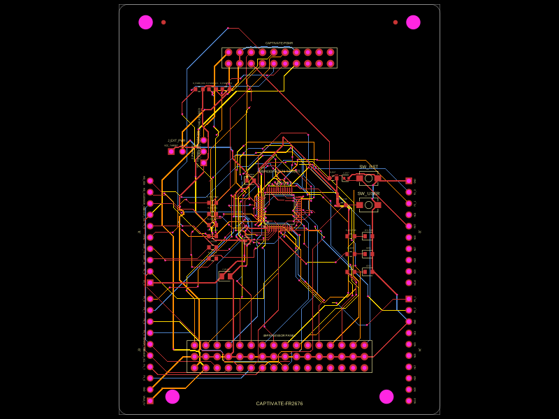
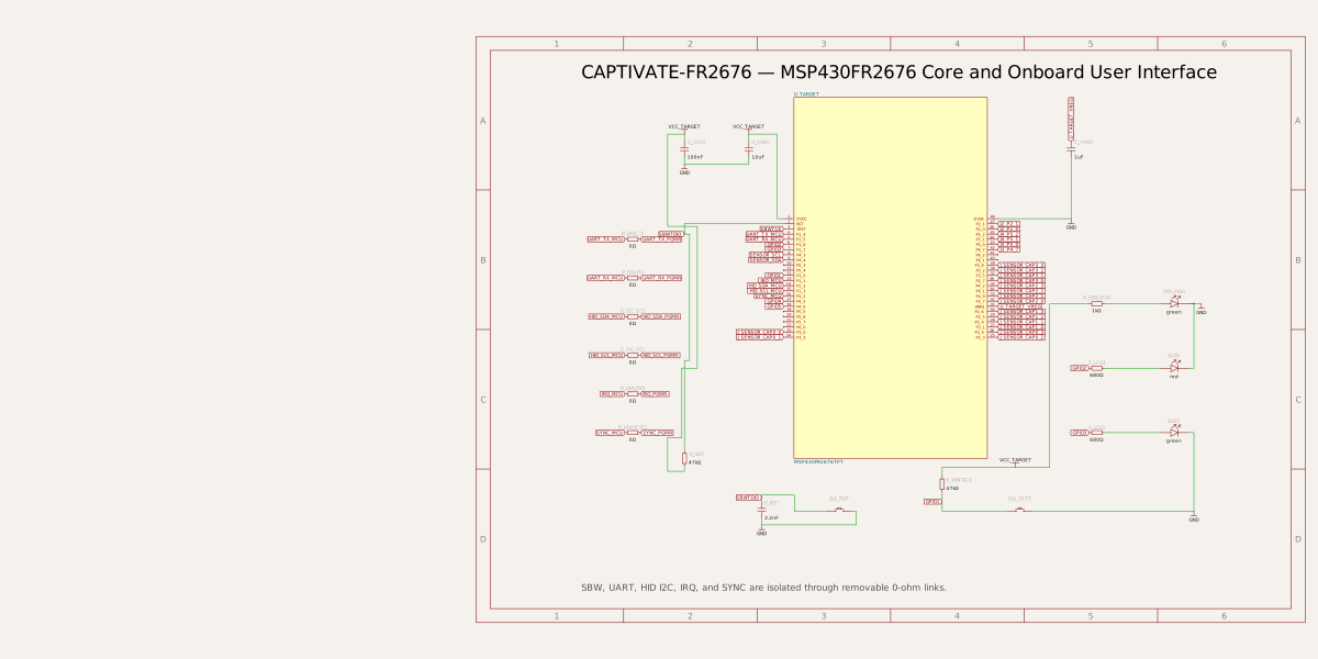
This circuit implements an MSP430FR2676 microcontroller-based development module with integrated power regulation, user interface components, programming interfaces, and sensor/boosterpack headers for embedded system prototyping.
- Version
- 1.0.0
- License
- unset
- Stars
- 0
index.circuit.tsx
PCB
Schematic
import { MSP430FR2676TPT } from "./imports/MSP430FR2676TPT"
import { TS342A2P_WZ } from "./imports/TS342A2P_WZ"

const onSheet = <const T extends Record<string, unknown>>(
  schSheetName: string,
  placement: T,
) => ({ schSheetName, ...placement })

const SCH = {
  U_TARGET: onSheet("MCU", { schX: 0, schY: 2 }),
  C_DVCC: onSheet("MCU", { schX: -8, schY: 7, schOrientation: "vertical" }),
  C_BULK: onSheet("MCU", { schX: -5.5, schY: 7, schOrientation: "vertical" }),
  C_VREG: onSheet("MCU", { schX: 7, schY: 7, schOrientation: "vertical" }),
  R_RST: onSheet("MCU", { schX: -8, schY: -5, schOrientation: "vertical" }),
  C_RST: onSheet("MCU", { schX: -5, schY: -7, schOrientation: "vertical" }),
  SW_RST: onSheet("MCU", { schX: -2, schY: -7, schOrientation: "down" }),
  R_BUTTON: onSheet("MCU", { schX: 2, schY: -6, schOrientation: "vertical" }),
  SW_USER: onSheet("MCU", { schX: 5, schY: -7, schOrientation: "down" }),
  R_LED_PWR: onSheet("MCU", { schX: 8, schY: 1, schOrientation: "horizontal" }),
  LED_PWR: onSheet("MCU", { schX: 11, schY: 1, schOrientation: "horizontal" }),
  R_LED1: onSheet("MCU", { schX: 8, schY: -1.5, schOrientation: "horizontal" }),
  LED1: onSheet("MCU", { schX: 11, schY: -1.5, schOrientation: "horizontal" }),
  R_LED2: onSheet("MCU", { schX: 8, schY: -4, schOrientation: "horizontal" }),
  LED2: onSheet("MCU", { schX: 11, schY: -4, schOrientation: "horizontal" }),
  R_TX: onSheet("MCU", { schX: -10, schY: 3.5, schOrientation: "horizontal" }),
  R_RX: onSheet("MCU", { schX: -10, schY: 2, schOrientation: "horizontal" }),
  R_SDA: onSheet("MCU", { schX: -10, schY: 0.5, schOrientation: "horizontal" }),
  R_SCL: onSheet("MCU", { schX: -10, schY: -1, schOrientation: "horizontal" }),
  R_IRQ: onSheet("MCU", { schX: -10, schY: -2.5, schOrientation: "horizontal" }),
  R_SYNC: onSheet("MCU", { schX: -10, schY: -4, schOrientation: "horizontal" }),
  J_PGMR: onSheet("INTERFACES", { schX: -10, schY: 3 }),
  J_PWRSEL: onSheet("INTERFACES", { schX: -10, schY: -6 }),
  J_EXT_PWR: onSheet("INTERFACES", { schX: -4, schY: -7 }),
  J_SENSOR: onSheet("INTERFACES", { schX: 4, schY: 2 }),
  J1: onSheet("INTERFACES", { schX: 8, schY: 7 }),
  J2: onSheet("INTERFACES", { schX: 8, schY: 2 }),
  J3: onSheet("INTERFACES", { schX: 8, schY: -3 }),
  J4: onSheet("INTERFACES", { schX: 8, schY: -8 }),
  R_PGMR_SDA: onSheet("INTERFACES", { schX: -4, schY: 5, schOrientation: "vertical" }),
  R_PGMR_SCL: onSheet("INTERFACES", { schX: -2, schY: 5, schOrientation: "vertical" }),
  R_PGMR_IRQ: onSheet("INTERFACES", { schX: 0, schY: 5, schOrientation: "vertical" }),
} as const

const targetFanout = (pin: number) => {
  const viaLayer: "inner1" | "inner2" = pin % 2 === 0 ? "inner1" : "inner2"
  if (pin <= 12) {
    return [{ x: -9.9 + (pin - 1) * 1.8, y: -9.5, via: true, to_layer: viaLayer }]
  }
  if (pin <= 24) {
    return [{ x: 9.5, y: -9.9 + (pin - 13) * 1.8, via: true, to_layer: viaLayer }]
  }
  if (pin <= 36) {
    return [{ x: 9.9 - (pin - 25) * 1.8, y: 9.5, via: true, to_layer: viaLayer }]
  }
  if (pin <= 48) {
    return [{ x: -9.5, y: 9.9 - (pin - 37) * 1.8, via: true, to_layer: viaLayer }]
  }
  return undefined
}

type PthPadProps = {
  pin: number
  x: number
  y: number
}

const PthPad = ({ pin, x, y }: PthPadProps) => (
  <platedhole
    portHints={[`pin${pin}`]}
    pcbX={`${x}mm`}
    pcbY={`${y}mm`}
    shape="circle"
    holeDiameter="0.9mm"
    outerDiameter="1.7mm"
  />
)

const ProgrammerConnector = (props: any) => {
  const labels = {
    pin1: "VCC_LDO",
    pin2: "VCC_MEASURED",
    pin3: "GND1",
    pin4: "GND2",
    pin5: "SBWTDIO",
    pin6: "SBWTCK",
    pin7: "UART_TX",
    pin8: "UART_RX",
    pin9: "HID_SDA",
    pin10: "HID_SCL",
    pin11: "IRQ",
    pin12: "SYNC",
    pin13: "VBUS_5V",
    pin14: "GND3",
    pin15: "NC15",
    pin16: "NC16",
    pin17: "NC17",
    pin18: "NC18",
    pin19: "NC19",
    pin20: "NC20",
  } as const

  return (
    <connector
      {...props}
      manufacturerPartNumber="CAPTIVATE-PGMR 2x10 female interface"
      pinLabels={labels}
      schPinArrangement={{
        leftSide: ["VCC_LDO", "VCC_MEASURED", "VBUS_5V", "GND1", "GND2", "GND3"],
        rightSide: ["SBWTDIO", "SBWTCK", "UART_TX", "UART_RX", "HID_SDA", "HID_SCL", "IRQ", "SYNC", "NC15", "NC16", "NC17", "NC18", "NC19", "NC20"],
      }}
      footprint={
        <footprint>
          {Array.from({ length: 10 }, (_, index) => (
            <PthPad key={`pgmr-a-${index}`} pin={index * 2 + 1} x={-11.43 + index * 2.54} y={-1.27} />
          ))}
          {Array.from({ length: 10 }, (_, index) => (
            <PthPad key={`pgmr-b-${index}`} pin={index * 2 + 2} x={-11.43 + index * 2.54} y={1.27} />
          ))}
          <silkscreenrect width="25.8mm" height="4.6mm" />
          <silkscreentext text="CAPTIVATE-PGMR" pcbX="0mm" pcbY="3.4mm" fontSize="0.7mm" />
        </footprint>
      }
    />
  )
}

const capLabels = [
  "CAP0_0", "CAP0_1", "CAP0_2", "CAP0_3",
  "CAP1_0", "CAP1_1", "CAP1_2", "CAP1_3",
  "CAP2_0", "CAP2_1", "CAP2_2", "CAP2_3",
  "CAP3_0", "CAP3_1", "CAP3_2", "CAP3_3",
] as const

const sensorLabels = {
  pin1: "CAP0_0", pin2: "CAP0_1", pin3: "CAP0_2", pin4: "CAP0_3",
  pin5: "CAP1_0", pin6: "CAP1_1", pin7: "CAP1_2", pin8: "CAP1_3",
  pin9: "CAP2_0", pin10: "CAP2_1", pin11: "CAP2_2", pin12: "CAP2_3",
  pin13: "CAP3_0", pin14: "CAP3_1", pin15: "CAP3_2", pin16: "CAP3_3",
  pin17: "GND01", pin18: "GND02", pin19: "GND03", pin20: "GND04",
  pin21: "GND05", pin22: "GND06", pin23: "GND07", pin24: "GND08",
  pin25: "GND09", pin26: "GND10", pin27: "GND11", pin28: "GND12",
  pin29: "GND13", pin30: "GND14", pin31: "GND15", pin32: "GND16",
  pin33: "VCC_3V3", pin34: "VBUS_5V", pin35: "SENSOR_SDA", pin36: "SENSOR_SCL",
  pin37: "GPIO1", pin38: "GPIO2", pin39: "GPIO3", pin40: "GPIO4", pin41: "GPIO5",
  pin42: "NC42", pin43: "NC43", pin44: "NC44", pin45: "NC45",
  pin46: "NC46", pin47: "NC47", pin48: "NC48",
} as const

const SensorConnector = (props: any) => (
  <connector
    {...props}
    manufacturerPartNumber="CapTIvate 3x16 sensor-panel connector"
    pinLabels={sensorLabels}
    schPinArrangement={{
      leftSide: ["VCC_3V3", "VBUS_5V", "SENSOR_SDA", "SENSOR_SCL", "GPIO1", "GPIO2", "GPIO3", "GPIO4", "GPIO5"],
      rightSide: [...capLabels, "GND01", "GND02", "GND03", "GND04", "GND05", "GND06", "GND07", "GND08", "GND09", "GND10", "GND11", "GND12", "GND13", "GND14", "GND15", "GND16", "NC42", "NC43", "NC44", "NC45", "NC46", "NC47", "NC48"],
    }}
    footprint={
      <footprint>
        {Array.from({ length: 16 }, (_, index) => (
          <PthPad key={`sensor-top-${index}`} pin={index + 1} x={-19.05 + index * 2.54} y={2.54} />
        ))}
        {Array.from({ length: 16 }, (_, index) => (
          <PthPad key={`sensor-gnd-${index}`} pin={index + 17} x={-19.05 + index * 2.54} y={0} />
        ))}
        {Array.from({ length: 16 }, (_, index) => (
          <PthPad key={`sensor-bottom-${index}`} pin={index + 33} x={-19.05 + index * 2.54} y={-2.54} />
        ))}
        <silkscreenrect width="41.5mm" height="7.2mm" />
        <silkscreentext text="48-PIN SENSOR PANEL" pcbX="0mm" pcbY="4.8mm" fontSize="0.7mm" />
      </footprint>
    }
  />
)

const CapTrace = ({ index }: { index: number }) => {
  const label = capLabels[index]
  const pin = index < 4 ? 23 + index
    : index < 8 ? 27 + (index - 4)
      : index < 12 ? 32 + (index - 8)
        : 36 + (index - 12)
  return (
    <trace
      from={`U_TARGET.${label}`}
      to={`J_SENSOR.${label}`}
      pcbRouteHints={targetFanout(pin)}
    />
  )
}

const SensorGroundTrace = ({ index }: { index: number }) => (
  <trace from={`J_SENSOR.GND${String(index + 1).padStart(2, "0")}`} to="net.GND" />
)

export default () => (
  <board
    title="CAPTIVATE-FR2676 MSP430 CapTIvate module - tscircuit edition"
    width="72mm"
    height="92mm"
    layers={4}
    borderRadius="2mm"
    minTraceWidth="0.15mm"
    minViaHoleDiameter="0.3mm"
    minViaPadDiameter="0.45mm"
    pcbStyle={{ viaHoleDiameter: "0.3mm", viaPadDiameter: "0.45mm" }}
    autorouter={{ preset: "default", allowViaInPad: false }}
  >
    <schematicsheet name="MCU" displayName="MSP430FR2676 Core, Power, and User Interface" sheetIndex={0}>
      <schematictext text="CAPTIVATE-FR2676 — MSP430FR2676 Core and Onboard User Interface" schX={-12} schY={10} fontSize={0.7} anchor="left" />
      <schematictext text="SBW, UART, HID I2C, IRQ, and SYNC are isolated through removable 0-ohm links." schX={-12} schY={-10} fontSize={0.35} anchor="left" color="#555555" />
    </schematicsheet>
    <schematicsheet name="INTERFACES" displayName="PGMR, Sensor Panel, and BoosterPack Headers" sheetIndex={1}>
      <schematictext text="CAPTIVATE-PGMR, 48-pin Sensor Panel, and Limited BoosterPack Interface" schX={-12} schY={10} fontSize={0.7} anchor="left" />
      <schematictext text="J_PWRSEL pins 1-2: normal VCC_LDO; pins 2-3: EnergyTrace VCC_MEASURED." schX={-12} schY={-10} fontSize={0.35} anchor="left" color="#555555" />
    </schematicsheet>

    <hole name="H1" diameter="3.2mm" pcbX={-30} pcbY={42} />
    <hole name="H2" diameter="3.2mm" pcbX={30} pcbY={42} />
    <hole name="H3" diameter="3.2mm" pcbX={-24} pcbY={-42} />
    <hole name="H4" diameter="3.2mm" pcbX={24} pcbY={-42} />
    <fiducial name="FID1" padDiameter="1mm" soldermaskPullback="1mm" pcbX={-26} pcbY={42} />
    <fiducial name="FID2" padDiameter="1mm" soldermaskPullback="1mm" pcbX={26} pcbY={42} />
    <silkscreentext text="CAPTIVATE-FR2676" fontSize="1.1mm" pcbX={0} pcbY={-43.5} />
    <silkscreentext text="MSP430FR2676 TARGET" fontSize="0.8mm" pcbX={0} pcbY={8.5} />
    <silkscreentext text="J_PWRSEL: LDO-TARGET-MEASURED" fontSize="0.62mm" pcbX={-18} pcbY={17} pcbRotation={90} />

    <ProgrammerConnector
      name="J_PGMR"
      {...SCH.J_PGMR}
      schWidth="7mm"
      schHeight="12mm"
      pcbX={0}
      pcbY={34}
      noConnect={["NC15", "NC16", "NC17", "NC18", "NC19", "NC20"]}
    />
    <SensorConnector
      name="J_SENSOR"
      {...SCH.J_SENSOR}
      schWidth="8mm"
      schHeight="18mm"
      pcbX={0}
      pcbY={-33}
      noConnect={["NC42", "NC43", "NC44", "NC45", "NC46", "NC47", "NC48"]}
    />

    <pinheader
      name="J_PWRSEL"
      {...SCH.J_PWRSEL}
      pinCount={3}
      gender="male"
      pitch="2.54mm"
      footprint="pinrow3_p2.54mm"
      pinLabels={["VCC_LDO", "VCC_TARGET", "VCC_MEASURED"]}
      showSilkscreenPinLabels={true}
      pcbX={-17}
      pcbY={13}
      pcbRotation={90}
    />
    <pinheader
      name="J_EXT_PWR"
      {...SCH.J_EXT_PWR}
      pinCount={2}
      gender="male"
      pitch="2.54mm"
      footprint="pinrow2_p2.54mm"
      pinLabels={["VCC_TARGET", "GND"]}
      showSilkscreenPinLabels={true}
      pcbX={-23}
      pcbY={13}
    />

    <MSP430FR2676TPT
      name="U_TARGET"
      {...SCH.U_TARGET}
      schWidth="7.5mm"
      schHeight="14mm"
      pcbX={0}
      pcbY={0}
      noConnect={["P5_3", "P5_4", "P5_5", "P5_6", "P5_7", "P6_0", "P6_1", "P6_2"]}
      pinAttributes={{
        DVCC: { requiresPower: true },
        DVSS: { requiresGround: true },
        VREG: { mustBeConnected: true },
      }}
    />
    <capacitor name="C_DVCC" {...SCH.C_DVCC} capacitance="100nF" maxDecouplingTraceLength="100mm" footprint="0402" pcbX={-7} pcbY={-7} />
    <capacitor name="C_BULK" {...SCH.C_BULK} capacitance="10uF" maxDecouplingTraceLength="25mm" footprint="0805" pcbX={-12} pcbY={-15} />
    <capacitor name="C_VREG" {...SCH.C_VREG} capacitance="1uF" maxDecouplingTraceLength="100mm" footprint="0603" pcbX={-6.5} pcbY={6.5} />
    <resistor name="R_RST" {...SCH.R_RST} resistance="47kohm" footprint="0603" pcbX={12} pcbY={7} />
    <capacitor name="C_RST" {...SCH.C_RST} capacitance="2.2nF" footprint="0402" pcbX={15} pcbY={7} />
    <TS342A2P_WZ name="SW_RST" {...SCH.SW_RST} pcbX={20} pcbY={7} />
    <resistor name="R_BUTTON" {...SCH.R_BUTTON} resistance="47kohm" footprint="0603" pcbX={14} pcbY={1} />
    <TS342A2P_WZ name="SW_USER" {...SCH.SW_USER} pcbX={20} pcbY={1} />

    <resistor name="R_LED_PWR" {...SCH.R_LED_PWR} resistance="1kohm" footprint="0603" pcbX={16} pcbY={-6} />
    <led name="LED_PWR" {...SCH.LED_PWR} color="green" footprint="0603" pcbX={20} pcbY={-6} />
    <resistor name="R_LED1" {...SCH.R_LED1} resistance="680ohm" footprint="0603" pcbX={16} pcbY={-10} />
    <led name="LED1" {...SCH.LED1} color="red" footprint="0603" pcbX={20} pcbY={-10} />
    <resistor name="R_LED2" {...SCH.R_LED2} resistance="680ohm" footprint="0603" pcbX={16} pcbY={-14} />
    <led name="LED2" {...SCH.LED2} color="green" footprint="0603" pcbX={20} pcbY={-14} />

    <resistor name="R_ISO_TX" {...SCH.R_TX} resistance="0ohm" footprint="0603" pcbX={-15} pcbY={-11} />
    <resistor name="R_ISO_RX" {...SCH.R_RX} resistance="0ohm" footprint="0603" pcbX={-15} pcbY={-8.5} />
    <resistor name="R_ISO_SDA" {...SCH.R_SDA} resistance="0ohm" footprint="0603" pcbX={-15} pcbY={-6} />
    <resistor name="R_ISO_SCL" {...SCH.R_SCL} resistance="0ohm" footprint="0603" pcbX={-15} pcbY={-3.5} />
    <resistor name="R_ISO_IRQ" {...SCH.R_IRQ} resistance="0ohm" footprint="0603" pcbX={-15} pcbY={-1} />
    <resistor name="R_ISO_SYNC" {...SCH.R_SYNC} resistance="0ohm" footprint="0603" pcbX={-15} pcbY={1.5} />
    <resistor name="R_PGMR_SDA" {...SCH.R_PGMR_SDA} resistance="4.7kohm" footprint="0603" pcbX={-18} pcbY={27} />
    <resistor name="R_PGMR_SCL" {...SCH.R_PGMR_SCL} resistance="4.7kohm" footprint="0603" pcbX={-15} pcbY={27} />
    <resistor name="R_PGMR_IRQ" {...SCH.R_PGMR_IRQ} resistance="4.7kohm" footprint="0603" pcbX={-12} pcbY={27} />

    <pinheader name="J1" {...SCH.J1} pinCount={10} gender="female" pitch="2.54mm" footprint="pinrow10_p2.54mm" pinLabels={["V3_3", "P1_0", "UART_RX", "UART_TX", "SYNC", "P1_6", "SENSOR_SCL", "SENSOR_SDA", "HID_SCL", "HID_SDA"]} showSilkscreenPinLabels={true} pcbX={-29} pcbY={-5} pcbRotation={90} />
    <connector name="J2" {...SCH.J2} manufacturerPartNumber="Limited BoosterPack right header" footprint="pinrow10_p2.54mm" pinLabels={{ pin1: "GND", pin2: "P2_0", pin3: "P2_1", pin4: "NC4", pin5: "RST", pin6: "NC6", pin7: "NC7", pin8: "NC8", pin9: "NC9", pin10: "NC10" }} noConnect={["NC4", "NC6", "NC7", "NC8", "NC9", "NC10"]} schPinArrangement={{ rightSide: ["GND", "P2_0", "P2_1", "NC4", "RST", "NC6", "NC7", "NC8", "NC9", "NC10"] }} pcbX={29} pcbY={-5} pcbRotation={270} />
    <pinheader name="J3" {...SCH.J3} pinCount={10} gender="female" pitch="2.54mm" footprint="pinrow10_p2.54mm" pinLabels={["VBUS_5V", "GND", "P1_6", "P1_7", "SENSOR_SCL", "SENSOR_SDA", "P4_5", "P4_6", "P4_7", "P5_0"]} showSilkscreenPinLabels={true} pcbX={-29} pcbY={-31.5} pcbRotation={90} />
    <connector name="J4" {...SCH.J4} manufacturerPartNumber="Limited BoosterPack right header" footprint="pinrow10_p2.54mm" pinLabels={{ pin1: "P5_1", pin2: "P5_2", pin3: "GND", pin4: "NC4", pin5: "NC5", pin6: "NC6", pin7: "NC7", pin8: "NC8", pin9: "NC9", pin10: "NC10" }} noConnect={["NC4", "NC5", "NC6", "NC7", "NC8", "NC9", "NC10"]} schPinArrangement={{ rightSide: ["P5_1", "P5_2", "GND", "NC4", "NC5", "NC6", "NC7", "NC8", "NC9", "NC10"] }} pcbX={29} pcbY={-31.5} pcbRotation={270} />

    <trace from="U_TARGET.DVCC" to="C_DVCC.pin1" pcbRouteHints={targetFanout(1)} thickness="0.3mm" />
    <trace from="U_TARGET.DVSS" to="C_DVCC.pin2" pcbRouteHints={targetFanout(48)} thickness="0.3mm" />
    <trace from="U_TARGET.VREG" to="C_VREG.pin1" pcbRouteHints={targetFanout(31)} />
    <trace from="C_VREG.pin2" to="U_TARGET.DVSS" />
    <trace from="C_DVCC.pin1" to="net.VCC_TARGET" thickness="0.3mm" />
    <trace from="C_DVCC.pin2" to="net.GND" />
    <trace from="C_BULK.pin1" to="net.VCC_TARGET" thickness="0.3mm" />
    <trace from="C_BULK.pin2" to="net.GND" />

    <trace from="U_TARGET.RST" to="net.SBWTDIO" pcbRouteHints={targetFanout(2)} />
    <trace from="U_TARGET.TEST" to="net.SBWTCK" pcbRouteHints={targetFanout(3)} />
    <trace from="R_RST.pin1" to="net.SBWTDIO" />
    <trace from="R_RST.pin2" to="net.VCC_TARGET" />
    <trace from="C_RST.pin1" to="net.SBWTDIO" />
    <trace from="C_RST.pin2" to="net.GND" />
    <trace from="SW_RST.pin1" to="net.SBWTDIO" />
    <trace from="SW_RST.pin2" to="net.GND" />

    <trace from="U_TARGET.USER_BUTTON" to="net.GPIO1" pcbRouteHints={targetFanout(12)} />
    <trace from="R_BUTTON.pin1" to="net.VCC_TARGET" />
    <trace from="R_BUTTON.pin2" to="net.GPIO1" />
    <trace from="SW_USER.pin1" to="net.GPIO1" />
    <trace from="SW_USER.pin2" to="net.GND" />

    <trace from="R_LED_PWR.pin1" to="net.VCC_TARGET" />
    <trace from="R_LED_PWR.pin2" to="LED_PWR.anode" />
    <trace from="LED_PWR.cathode" to="net.GND" />
    <trace from="U_TARGET.P1_6" to="net.GPIO2" pcbRouteHints={targetFanout(6)} />
    <trace from="R_LED1.pin1" to="net.GPIO2" />
    <trace from="R_LED1.pin2" to="LED1.anode" />
    <trace from="LED1.cathode" to="net.GND" />
    <trace from="U_TARGET.P1_7" to="net.GPIO3" pcbRouteHints={targetFanout(7)} />
    <trace from="R_LED2.pin1" to="net.GPIO3" />
    <trace from="R_LED2.pin2" to="LED2.anode" />
    <trace from="LED2.cathode" to="net.GND" />

    <trace from="U_TARGET.UART_TX" to="net.UART_TX_MCU" pcbRouteHints={targetFanout(4)} />
    <trace from="R_ISO_TX.pin1" to="net.UART_TX_MCU" />
    <trace from="R_ISO_TX.pin2" to="net.UART_TX_PGMR" />
    <trace from="U_TARGET.UART_RX" to="net.UART_RX_MCU" pcbRouteHints={targetFanout(5)} />
    <trace from="R_ISO_RX.pin1" to="net.UART_RX_MCU" />
    <trace from="R_ISO_RX.pin2" to="net.UART_RX_PGMR" />
    <trace from="U_TARGET.HID_SDA" to="net.HID_SDA_MCU" pcbRouteHints={targetFanout(14)} />
    <trace from="R_ISO_SDA.pin1" to="net.HID_SDA_MCU" />
    <trace from="R_ISO_SDA.pin2" to="net.HID_SDA_PGMR" />
    <trace from="U_TARGET.HID_SCL" to="net.HID_SCL_MCU" pcbRouteHints={targetFanout(15)} />
    <trace from="R_ISO_SCL.pin1" to="net.HID_SCL_MCU" />
    <trace from="R_ISO_SCL.pin2" to="net.HID_SCL_PGMR" />
    <trace from="U_TARGET.IRQ" to="net.IRQ_MCU" pcbRouteHints={targetFanout(13)} />
    <trace from="R_ISO_IRQ.pin1" to="net.IRQ_MCU" />
    <trace from="R_ISO_IRQ.pin2" to="net.IRQ_PGMR" />
    <trace from="U_TARGET.SYNC" to="net.SYNC_MCU" pcbRouteHints={targetFanout(16)} />
    <trace from="R_ISO_SYNC.pin1" to="net.SYNC_MCU" />
    <trace from="R_ISO_SYNC.pin2" to="net.SYNC_PGMR" />

    <trace from="J_PGMR.VCC_LDO" to="net.VCC_LDO" thickness="0.3mm" />
    <trace from="J_PGMR.VCC_MEASURED" to="net.VCC_MEASURED" thickness="0.3mm" />
    <trace from="J_PGMR.VBUS_5V" to="net.VBUS_5V" thickness="0.3mm" />
    <trace from="J_PGMR.GND1" to="net.GND" /><trace from="J_PGMR.GND2" to="net.GND" /><trace from="J_PGMR.GND3" to="net.GND" />
    <trace from="J_PGMR.SBWTDIO" to="net.SBWTDIO" />
    <trace from="J_PGMR.SBWTCK" to="net.SBWTCK" />
    <trace from="J_PGMR.UART_TX" to="net.UART_TX_PGMR" />
    <trace from="J_PGMR.UART_RX" to="net.UART_RX_PGMR" />
    <trace from="J_PGMR.HID_SDA" to="net.HID_SDA_PGMR" />
    <trace from="J_PGMR.HID_SCL" to="net.HID_SCL_PGMR" />
    <trace from="J_PGMR.IRQ" to="net.IRQ_PGMR" />
    <trace from="J_PGMR.SYNC" to="net.SYNC_PGMR" />
    <trace from="R_PGMR_SDA.pin1" to="net.HID_SDA_PGMR" /><trace from="R_PGMR_SDA.pin2" to="net.VCC_LDO" />
    <trace from="R_PGMR_SCL.pin1" to="net.HID_SCL_PGMR" /><trace from="R_PGMR_SCL.pin2" to="net.VCC_LDO" />
    <trace from="R_PGMR_IRQ.pin1" to="net.IRQ_PGMR" /><trace from="R_PGMR_IRQ.pin2" to="net.VCC_LDO" />

    <trace from="J_PWRSEL.VCC_LDO" to="net.VCC_LDO" thickness="0.3mm" />
    <trace from="J_PWRSEL.VCC_TARGET" to="net.VCC_TARGET" thickness="0.3mm" />
    <trace from="J_PWRSEL.VCC_MEASURED" to="net.VCC_MEASURED" thickness="0.3mm" />
    <trace from="J_EXT_PWR.VCC_TARGET" to="net.VCC_TARGET" thickness="0.3mm" />
    <trace from="J_EXT_PWR.GND" to="net.GND" thickness="0.3mm" />

    {capLabels.map((_, index) => <CapTrace key={`cap-trace-${index}`} index={index} />)}
    {Array.from({ length: 16 }, (_, index) => <SensorGroundTrace key={`sensor-ground-${index}`} index={index} />)}
    <trace from="J_SENSOR.VCC_3V3" to="net.VCC_LDO" thickness="0.3mm" />
    <trace from="J_SENSOR.VBUS_5V" to="net.VBUS_5V" thickness="0.3mm" />
    <trace from="U_TARGET.SENSOR_SCL" to="net.SENSOR_SCL" pcbRouteHints={targetFanout(8)} />
    <trace from="U_TARGET.SENSOR_SDA" to="net.SENSOR_SDA" pcbRouteHints={targetFanout(9)} />
    <trace from="J_SENSOR.SENSOR_SCL" to="net.SENSOR_SCL" />
    <trace from="J_SENSOR.SENSOR_SDA" to="net.SENSOR_SDA" />
    <trace from="J_SENSOR.GPIO1" to="net.GPIO1" />
    <trace from="J_SENSOR.GPIO2" to="net.GPIO2" />
    <trace from="J_SENSOR.GPIO3" to="net.GPIO3" />
    <trace from="U_TARGET.P4_5" to="net.GPIO4" pcbRouteHints={targetFanout(17)} />
    <trace from="J_SENSOR.GPIO4" to="net.GPIO4" />
    <trace from="U_TARGET.P4_6" to="net.GPIO5" pcbRouteHints={targetFanout(18)} />
    <trace from="J_SENSOR.GPIO5" to="net.GPIO5" />

    <trace from="J1.V3_3" to="net.VCC_TARGET" /><trace from="J1.P1_0" to="net.GPIO1" />
    <trace from="J1.UART_RX" to="net.UART_RX_MCU" /><trace from="J1.UART_TX" to="net.UART_TX_MCU" />
    <trace from="J1.SYNC" to="net.SYNC_MCU" /><trace from="J1.P1_6" to="net.GPIO2" />
    <trace from="J1.SENSOR_SCL" to="net.SENSOR_SCL" /><trace from="J1.SENSOR_SDA" to="net.SENSOR_SDA" />
    <trace from="J1.HID_SCL" to="net.HID_SCL_MCU" /><trace from="J1.HID_SDA" to="net.HID_SDA_MCU" />
    <trace from="J2.GND" to="net.GND" />
    <trace from="U_TARGET.P2_0" to="J2.P2_0" pcbRouteHints={targetFanout(46)} />
    <trace from="U_TARGET.P2_1" to="J2.P2_1" pcbRouteHints={targetFanout(47)} />
    <trace from="J2.RST" to="net.SBWTDIO" />
    <trace from="J3.VBUS_5V" to="net.VBUS_5V" /><trace from="J3.GND" to="net.GND" />
    <trace from="J3.P1_6" to="net.GPIO2" /><trace from="J3.P1_7" to="net.GPIO3" />
    <trace from="J3.SENSOR_SCL" to="net.SENSOR_SCL" /><trace from="J3.SENSOR_SDA" to="net.SENSOR_SDA" />
    <trace from="J3.P4_5" to="net.GPIO4" /><trace from="J3.P4_6" to="net.GPIO5" />
    <trace from="U_TARGET.P4_7" to="J3.P4_7" pcbRouteHints={targetFanout(42)} />
    <trace from="U_TARGET.P5_0" to="J3.P5_0" pcbRouteHints={targetFanout(43)} />
    <trace from="U_TARGET.P5_1" to="J4.P5_1" pcbRouteHints={targetFanout(44)} />
    <trace from="U_TARGET.P5_2" to="J4.P5_2" pcbRouteHints={targetFanout(45)} />
    <trace from="J4.GND" to="net.GND" />
  </board>
)