ShiboSoftwareDev/am625sip-linux-board
This code defines the physical footprint and pin layout for an AM625 System-in-Package (SIP) component, detailing pad positions, pin labels, and package outline for hardware integration.
- Version
- 1.0.24
- License
- unset
- Stars
- 0
subcircuits/cap-vdds.tsx
import { Fragment } from "react"

export const CAP_VDDS_LINKS = [
  { ball: "G9", name: "C44", exitX: -1, exitY: 10, portX: -1, portY: 10, parentLayer: "inner2", capX: -1, capY: 13.26, rotation: 90, layer: "top" },
  { ball: "H11", name: "C45", exitX: 0.5, exitY: 10, portX: 0.5, portY: 10, parentLayer: "inner2", capX: 1.5, capY: 13.26, rotation: 90, layer: "top" },
  { ball: "H15", name: "C46", exitX: 1, exitY: 10, portX: 1, portY: 10, parentLayer: "inner2", capX: 4, capY: 13.26, rotation: 90, layer: "top" },
  { ball: "H17", name: "C47", exitX: 6.47404, exitY: 10, portX: 6.47404, portY: 10, parentLayer: "inner2", capX: 4.5, capY: 13.26, rotation: 270, layer: "bottom" },
  { ball: "J19", name: "C48", exitX: 12, exitY: 1.5, portX: 12, portY: 1.5, parentLayer: "inner1", capX: 15.26, capY: 1.5, rotation: 0, layer: "top" },
  { ball: "K18", name: "C49", exitX: 12, exitY: -0.75, portX: 12, portY: -0.75, parentLayer: "inner1", capX: 17, capY: -0.75, rotation: 0, layer: "top" },
  { ball: "P19", name: "C50", exitX: 12, exitY: -4, portX: 12, portY: -4, parentLayer: "inner1", capX: 12, capY: -7.26, rotation: 270, layer: "bottom" },
  { ball: "U7", name: "C51", exitX: -4.5, exitY: -12.9999, portX: -4.5, portY: -12.9999, parentLayer: "bottom", capX: -4.5, capY: -16.2599, rotation: 270, layer: "top" },
  { ball: "W17", name: "C52", exitX: 2.75, exitY: -12.9999, portX: 2.75, portY: -12.9999, parentLayer: "bottom", capX: 2.75, capY: -16.2599, rotation: 270, layer: "top" },
] as const

const BoundaryVia = ({ name, pcbX, pcbY }: {
  name: string
  pcbX: number
  pcbY: number
}) => (
  <chip
    name={name}
    pcbX={pcbX}
    pcbY={pcbY}
    noSchematicRepresentation
    footprint={
      <footprint>
        <platedhole
          portHints={["pin1"]}
          shape="circle"
          holeDiameter="0.1mm"
          outerDiameter="0.24mm"
        />
      </footprint>
    }
  />
)

export const CapVddsSubcircuit = () => (
  <subcircuit
    name="CAP_VDDS"
    pcbX={0}
    pcbY={0}
    autorouter="default"
    exposedNets={["GND"]}
  >
    <autoroutingphase
      name="CAP_VDDS_GROUND_DROPS"
      phaseIndex={0}
      autorouter="fanout"
      fanoutRoutingLayers={["top", "inner1", "inner2", "bottom"]}
      fanoutPourNetMap={{ inner1: ["GND"] }}
    />
    {CAP_VDDS_LINKS.map(({ ball }, index) => (
      <autoroutingphase
        key={`CAP_VDDS_LOCAL_LINK_${ball}`}
        name={`CAP_VDDS_LOCAL_LINK_${ball}`}
        phaseIndex={index + 1}
        autorouter="default"
      />
    ))}

    <net name="GND" routingPhaseIndex={0} />
    {CAP_VDDS_LINKS.map(
      ({ ball, name, portX, portY, capX, capY, rotation, layer }, index) => (
        <Fragment key={`${ball}-${name}`}>
          <BoundaryVia
            name={`X_${ball}`}
            pcbX={portX}
            pcbY={portY}
          />
          <capacitor
            name={name}
            capacitance="1uF"
            maxVoltageRating="10V"
            footprint="0402"
            supplierPartNumbers={{ jlcpcb: ["C52923"] }}
            pcbX={capX}
            pcbY={capY}
            pcbRotation={rotation}
            layer={layer}
          />
          <trace
            name={`CAP_VDDS_INTERNAL_${ball}`}
            from={`.X_${ball} > .pin1`}
            to={`.${name} > .pin1`}
            routingPhaseIndex={index + 1}
            maxLength="6mm"
          />
          <trace
            name={`CAP_VDDS_GROUND_${ball}`}
            from={`.${name} > .pin2`}
            to="net.GND"
            routingPhaseIndex={0}
            maxLength="10mm"
          />
        </Fragment>
      ),
    )}
  </subcircuit>
)
Related Packages
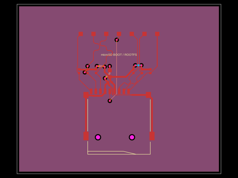 More from this authorShiboSoftwareDev/t113-s3-linux-computer-p9The code defines a PCB subcircuit for a buck converter module featuring a TMI3112H IC, FTC252010S power switch, and associated passive components like capacitors and resistors for voltage regulation and feedback control.
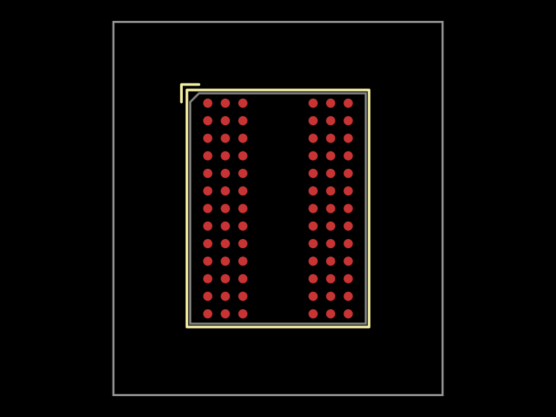 Similar package0hmX/mt41k512m8da-107-it-p-footprintsThis code defines the mechanical and physical layout of a Micron digital ball grid array (FBGA) package with 78 balls, including pin positions, footprint geometry, PCB pads, and silkscreen outlines for surface-mount integration.
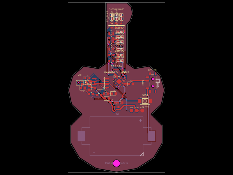 Discover something newgokul/acoustic-guitar-tunerThis code defines a miniature circuit board featuring a microcontroller (ATTINY1616-MNR), audio and power components, tactile switch, various LEDs, and passive components arranged with specific footprints, connections, and mechanical markings for a mini acoustic guitar tuner.