ShiboSoftwareDev/am625sip-linux-board
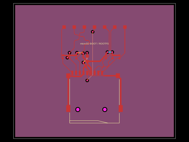
This code defines the physical footprint and pin layout for an AM625 System-in-Package (SIP) component, detailing pad positions, pin labels, and package outline for hardware integration.
- Version
- 1.0.24
- License
- unset
- Stars
- 0
imports/TF_01A.tsx
import type { ChipProps } from "@tscircuit/props"

const pinLabels = {
  pin1: ["pin1"],
  pin2: ["pin2"],
  pin3: ["pin3"],
  pin4: ["VDD"],
  pin5: ["pin5"],
  pin6: ["VSS"],
  pin7: ["pin7"],
  pin8: ["pin8"],
  pin9: ["CD"],
  pin10: ["GND1"],
  pin11: ["GND4"],
  pin12: ["GND3"],
  pin13: ["GND2"]
} as const

export const TF_01A = (props: ChipProps<typeof pinLabels>) => {
  return (
    <chip
      pinLabels={pinLabels}
      supplierPartNumbers={{
  "jlcpcb": [
    "C91145"
  ]
}}
      manufacturerPartNumber="TF_01A"
      footprint={<footprint>
        <hole pcbX="-4.9499393mm" pcbY="-5.39108015mm" diameter="0.999998mm" />
<hole pcbX="3.0500447mm" pcbY="-5.39108015mm" diameter="0.999998mm" />
<smtpad portHints={["pin1"]} pcbX="2.2400133mm" pcbY="5.45108765mm" width="0.5999988mm" height="1.2999974mm" shape="rect" />
<smtpad portHints={["pin2"]} pcbX="1.1399647mm" pcbY="5.45108765mm" width="0.5999988mm" height="1.2999974mm" shape="rect" />
<smtpad portHints={["pin3"]} pcbX="0.0399161mm" pcbY="5.45108765mm" width="0.5999988mm" height="1.2999974mm" shape="rect" />
<smtpad portHints={["pin4"]} pcbX="-1.0601325mm" pcbY="5.45108765mm" width="0.5999988mm" height="1.2999974mm" shape="rect" />
<smtpad portHints={["pin5"]} pcbX="-2.1599525mm" pcbY="5.45108765mm" width="0.5999988mm" height="1.2999974mm" shape="rect" />
<smtpad portHints={["pin6"]} pcbX="-3.2600011mm" pcbY="5.45108765mm" width="0.5999988mm" height="1.2999974mm" shape="rect" />
<smtpad portHints={["pin7"]} pcbX="-4.3600497mm" pcbY="5.45108765mm" width="0.5999988mm" height="1.2999974mm" shape="rect" />
<smtpad portHints={["pin8"]} pcbX="-5.4598697mm" pcbY="5.45108765mm" width="0.5999988mm" height="1.2999974mm" shape="rect" />
<smtpad portHints={["pin9"]} pcbX="-6.5599691mm" pcbY="5.45068125mm" width="0.5999988mm" height="1.2999974mm" shape="rect" />
<smtpad portHints={["pin10"]} pcbX="-7.7599667mm" pcbY="4.60069565mm" width="1.1999976mm" height="1.3999972mm" shape="rect" />
<smtpad portHints={["pin13"]} pcbX="6.9200141mm" pcbY="4.60069565mm" width="1.1999976mm" height="1.3999972mm" shape="rect" />
<smtpad portHints={["pin12"]} pcbX="7.7599667mm" pcbY="-5.10108835mm" width="1.1999976mm" height="1.999996mm" shape="rect" />
<smtpad portHints={["pin11"]} pcbX="-7.7599667mm" pcbY="-5.10108835mm" width="1.1999976mm" height="1.999996mm" shape="rect" />
<silkscreenpath route={[{"x":-7.365987300000029,"y":3.581139650000182},{"x":-7.365987300000029,"y":-3.927989349999848}]} />
<silkscreenpath route={[{"x":7.366012699999828,"y":-3.991514749999851},{"x":7.366012699999828,"y":3.501485250000087}]} />
<silkscreenpath route={[{"x":-7.365987300000029,"y":-6.340963949999946},{"x":-7.365987300000029,"y":-9.401054349999981},{"x":7.366012699999828,"y":-9.401028949999954},{"x":7.366012699999828,"y":-6.491027149999923}]} />
<silkscreenpath route={[{"x":-7.365987300000029,"y":-8.915685749999966},{"x":-7.365987300000029,"y":-8.691022750000116},{"x":1.000010699999848,"y":-8.691022750000116},{"x":3.9370126999999684,"y":-9.388100349999945}]} />
<silkscreentext text="{NAME}" pcbX="0.0000127mm" pcbY="7.11097965mm" anchorAlignment="center" fontSize="1mm" />
<courtyardoutline outline={[{"x":-8.606587300000115,"y":6.360979650000104},{"x":8.606612699999914,"y":6.360979650000104},{"x":8.606612699999914,"y":-9.73462035},{"x":-8.606587300000115,"y":-9.73462035},{"x":-8.606587300000115,"y":6.360979650000104}]} />
      </footprint>}
      cadModel={{
        objUrl: "https://modelcdn.tscircuit.com/easyeda_models/assets/C91145.obj?uuid=5685a23adc9a4e3e9b914abe5ae03aae",
        stepUrl: "https://modelcdn.tscircuit.com/easyeda_models/assets/C91145.step?uuid=5685a23adc9a4e3e9b914abe5ae03aae",
        pcbRotationOffset: 0,
        modelOriginPosition: { x: -0.0022224999997728645, y: 5.101310850000045, z: -0.14733820000000009 },
      }}
      {...props}
    />
  )
}
Related Packages
 More from this authorShiboSoftwareDev/t113-s3-linux-computer-p9The code defines a PCB subcircuit for a buck converter module featuring a TMI3112H IC, FTC252010S power switch, and associated passive components like capacitors and resistors for voltage regulation and feedback control.
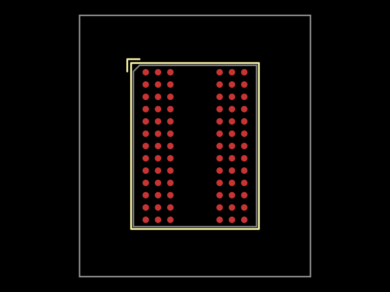 Similar package0hmX/mt41k512m8da-107-it-p-footprintsThis code defines the mechanical and physical layout of a Micron digital ball grid array (FBGA) package with 78 balls, including pin positions, footprint geometry, PCB pads, and silkscreen outlines for surface-mount integration.
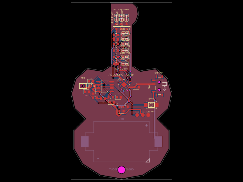 Discover something newgokul/acoustic-guitar-tunerThis code defines a miniature circuit board featuring a microcontroller (ATTINY1616-MNR), audio and power components, tactile switch, various LEDs, and passive components arranged with specific footprints, connections, and mechanical markings for a mini acoustic guitar tuner.