Niharika0104/AND-Circuit-Board
A tscircuit package created by Niharika0104.
Usage: To import and use the "@tsci/Niharika0104.XD74LS08_AND_CHIP" component: 1. Import the component: ```tsx import { useXD74LS08 } from "@tsci/Niharika0104.XD74LS08_AND_CHIP" ``` 2. Use the component in your circuit: ```tsx const U1 = useXD74LS08("U1") <U1 pcbX={0} pcbY={2} schX={8} schY={0} VCC="net.VBUS" GND="net.GND" /> ``` The component provides these pins: - A1, B1: First AND gate inputs - Y1: First AND gate output - A2, B2: Second AND gate inputs - Y2: Second AND gate output - A3, B3: Third AND gate inputs - Y3: Third AND gate output - A4, B4: Fourth AND gate inputs - Y4: Fourth AND gate output - VCC: Power supply - GND: Ground
- Version
- 0.0.1
- License
- unset
- Stars
- 0
index.ts
PCB
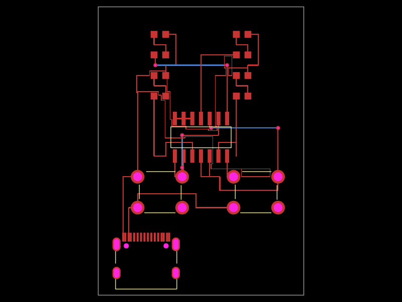
Schematic

import { useXD74LS08 } from "@tsci/Niharika0104.XD74LS08_AND_CHIP";
import { useUsbC } from "@tsci/seveibar.smd-usb-c";
import { usePushButton } from "@tsci/seveibar.push-button";
import { useResistor,useLed } from "@tscircuit/core";

export default () => {

  const U1 = useXD74LS08("U1");
  const USBC = useUsbC("USBC");
  const Button1 = usePushButton("SW1");
  const Button2 = usePushButton("SW2");
  const R1 = useResistor("R1", {
    resistance: "1k",
    footprint: "0603",
  });
  const R2 = useResistor("R2", {
    resistance: "1k",
    footprint: "0603",
  });
  const R3 = useResistor("R3", {
    resistance: "1k",
    footprint: "0603",
  });
  const R4 = useResistor("R4", {
    resistance: "1k",
    footprint: "0603",
  });
  const LED1 = useLed("LED1", { footprint: "0603" });
  const LED2 = useLed("LED2", { footprint: "0603" });
  const LED3 = useLed("LED3", { footprint: "0603" });
  const LED4 = useLed("LED4", { footprint: "0603" });

  return (
   <board width="30mm" height="42mm">

      <U1 pcbX={0} pcbY={2} schX={8} schY={0} VCC="net.VBUS" GND="net.GND"/>
      <USBC GND1="net.GND" pcbX={-8} pcbY={-15} VBUS1="net.VBUS" schX={0} schY={0} />

      <Button1 pcbX={-6} pcbY={-6} schX={5} schY={-5}  pin3="net.VBUS" pin1="net.GND"/>
      <Button2 pcbX={8} pcbY={-6} schX={5} schY={5} pin3="net.VBUS" pin1="net.GND"/>

      <R1 pcbX={-6} pcbY={8} schX={12} schY={-6}  left={U1.Y1}/>
      <LED1 pcbX={-6} pcbY={11} schX={14} schY={-6}  neg="net.GND" />

      <R2 pcbX={6} pcbY={8} schX={12} schY={-3} left={U1.Y2}/>
      <LED2 pcbX={6} pcbY={11} schX={14} schY={-3}  neg="net.GND"/>

      <R3 pcbX={-6} pcbY={14} schX={12} schY={0} left={U1.Y3} />
      <LED3 pcbX={-6} pcbY={17} schX={14} schY={0}  neg="net.GND" />

      <R4 pcbX={6} pcbY={14} schX={12} schY={3} left={U1.Y4} />
      <LED4 pcbX={6} pcbY={17} schX={14} schY={3}  neg="net.GND"/>

      {/* Connections to the inputs of the four AND gates on U1 */}
      <trace from={U1.A1} to=".SW1 > .pin2" />
      <trace from={U1.B1} to=".SW1 > .pin2" />
      <trace from={U1.A2} to=".SW2 > .pin2" />
      <trace from={U1.B2} to=".SW2 > .pin2" />
      <trace from={U1.A3} to=".SW1 > .pin2" />
      <trace from={U1.B3} to=".SW2 > .pin2" />
      <trace from={U1.A4} to="net.VBUS" />
      <trace from={U1.B4} to="net.VBUS" />

      {/* Connections from resistor outputs to the positive terminals of the LEDs */}
      <trace from={R1.pin2} to={LED1.pos} />
      <trace from={R2.pin2} to={LED2.pos} />
      <trace from={R3.pin2} to={LED3.pos} />
      <trace from={R4.pin2} to={LED4.pos} />

    </board>
  )
}