MustafaMulla29/unaligned-traces
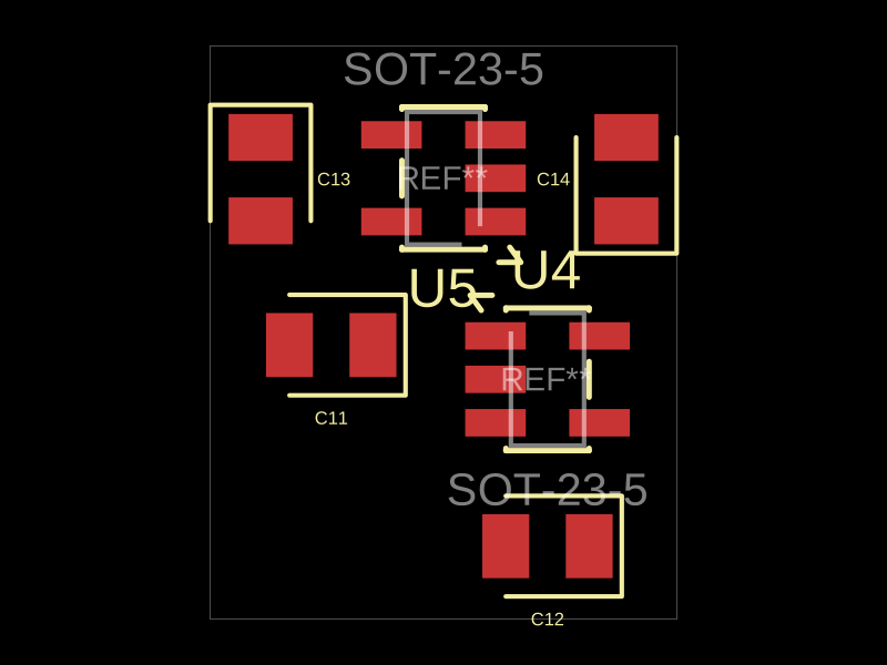
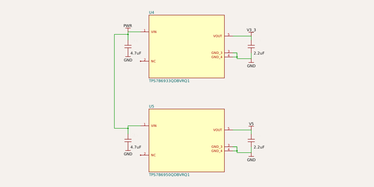
This code defines a SOT-23-5 package-based voltage regulator module with selectable 3.3V or 5V output, including pins for input (VIN), ground (GND), and output (VOUT), along with associated schematic symbols and circuit layout.
- Version
- 0.0.1
- License
- unset
- Stars
- 0
index.tsx
PCB
Schematic
import type { SubcircuitProps } from "@tscircuit/props";
import "tscircuit";
import {
  TPS7B6933QDBVRQ1,
  TPS7B6950QDBVRQ1,
} from "./TPS7B69QDBVRQ1.tsx";
import {
  type Tida01421AltiumOrigin,
  tida01421Position,
} from "./tida01421-coordinates.ts";

export const TIDA01421_POWER_ORIGIN: Tida01421AltiumOrigin = {
  x: 795,
  y: 360,
};

const p = (x: number, y: number) =>
  tida01421Position(x, y, TIDA01421_POWER_ORIGIN);

/**
 * Only the TIDA-01421 local 3.3 V and 5 V regulators required by the analog
 * chain. J3, D1, the ADCBAT monitor, D2, and LaunchPad circuitry are excluded.
 */
export const PinchDetectionPower_TPS7B69 = (props: SubcircuitProps) => (
  <subcircuit
    exposedNets={["PWR", "V3_3", "V5", "GND"]}
    schAutoLayoutEnabled={false}
    schMaxTraceDistance="20mm"
    routingDisabled
    {...props}
  >
    <net name="GND" isGroundNet />
    <net name="PWR" isPowerNet />
    <net name="V3_3" isPowerNet />
    <net name="V5" isPowerNet />

    <TPS7B6933QDBVRQ1 name="U4" noConnect={["NC"]} {...p(790, 440)} />
    <TPS7B6950QDBVRQ1 name="U5" noConnect={["NC"]} {...p(790, 280)} />
    <capacitor
      name="C11"
      capacitance="4.7uF"
      footprint="0805"
      schOrientation="vertical"
      {...p(690, 440)}
    />
    <capacitor
      name="C12"
      capacitance="2.2uF"
      footprint="0805"
      schOrientation="vertical"
      {...p(900, 440)}
    />
    <capacitor
      name="C13"
      capacitance="4.7uF"
      footprint="0805"
      schOrientation="vertical"
      {...p(690, 280)}
    />
    <capacitor
      name="C14"
      capacitance="2.2uF"
      footprint="0805"
      schOrientation="vertical"
      {...p(900, 280)}
    />

    <trace from="C11.pin1" to="U4.VIN" />
    <trace from="U4.VIN" to="U5.VIN" />
    <trace from="U5.VIN" to="C13.pin1" />
    <trace from="U4.VOUT" to="C12.pin1" />
    <trace from="U5.VOUT" to="C14.pin1" />
    <trace from="U4.GND_3" to="U4.GND_4" />
    <trace from="U4.GND_3" to="C12.pin2" />
    <trace from="U5.GND_3" to="U5.GND_4" />
    <trace from="U5.GND_3" to="C14.pin2" />

    <trace from="U4.VIN" to="net.PWR" />
    {/* Source V3.3 is normalized to V3_3 because native net identifiers reject
        periods. The component, value, placement, and electrical net are exact. */}
    <trace from="U4.VOUT" to="net.V3_3" />
    <trace from="U5.VOUT" to="net.V5" />
    <trace from="C11.pin2" to="net.GND"/>
    <trace from="C12.pin2" to="net.GND"/>
    <trace from="C13.pin2" to="net.GND"/>
    <trace from="C14.pin2" to="net.GND"/>

  </subcircuit>
);

export default PinchDetectionPower_TPS7B69;