MustafaMulla29/ti-boost-drv8848
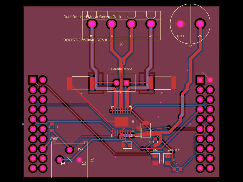
This code defines a hardware layout with 3D models, footprints, and schematic symbols for various electronic components including a potentiometer, motor driver ICs, connectors, capacitors, resistors, LEDs, and copper pours for ground overlays, assembled into a detailed schematic and PCB design.
- Version
- 1.0.1
- License
- unset
- Stars
- 0
index.circuit.tsx
PCB
Schematic
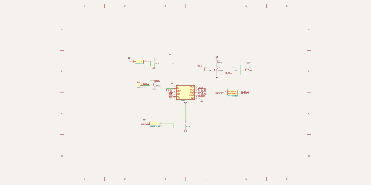
import { A_3386P_1_104TLF } from "./imports/A_3386P_1_104TLF";
import { DRV8848PWPR } from "./imports/DRV8848PWPR";
import { OSTTC022162 } from "./imports/OSTTC022162";
import { OSTTC042162 } from "./imports/OSTTC042162";

export default () => (
  <board
    title="TI BOOST-DRV8848 Dual Brushed Motor BoosterPack"
    width="50.8mm"
    height="44.45mm"
    layers={2}
    thickness="1.6mm"
    solderMaskColor="red"
    silkscreenColor="white"
    minViaHoleDiameter="0.3mm"
    minViaPadDiameter="0.45mm"
  >
    <schematicsheet
      name="Driver and motor power"
      displayName="Driver and motor power"
      sheetIndex={1}
    />
    <schematicsheet
      name="LaunchPad interface"
      displayName="LaunchPad interface"
      sheetIndex={2}
    />

    {/* TI BOM SLVC606, board revision A */}
    <DRV8848PWPR
      name="U1"
      schPinArrangement={{
        leftSide: {
          pins: [
            "VM",
            "VINT",
            "nSLEEP",
            "AIN1",
            "AIN2",
            "BIN1",
            "BIN2",
            "VREF",
          ],
          direction: "top-to-bottom",
        },
        rightSide: {
          pins: [
            "AOUT1",
            "AISEN",
            "AOUT2",
            "BOUT2",
            "BISEN",
            "BOUT1",
            "nFAULT",
            "GND",
            "PPAD",
          ],
          direction: "top-to-bottom",
        },
      }}
      pcbX={0}
      pcbY={-7.6454}
      pcbRotation={180}
      schX={0}
      schY={0}
      schWidth="2.34mm"
      schHeight="1.8mm"
      schSheetName="Driver and motor power"
    />

    <capacitor
      name="C1"
      capacitance="10uF"
      maxVoltageRating="35V"
      footprint="1206"
      manufacturerPartNumber="GMK316AB7106KL"
      pcbX={6.2484}
      pcbY={-9.4488}
      pcbRotation={90}
      schX={-4}
      schY={4}
      schOrientation="vertical"
      schSheetName="Driver and motor power"
    />
    <capacitor
      name="C2"
      capacitance="10nF"
      maxVoltageRating="100V"
      footprint="0603"
      manufacturerPartNumber="C1608X7R2A103K"
      pcbX={4.3434}
      pcbY={-10.0838}
      pcbRotation={90}
      schX={-2}
      schY={4}
      schOrientation="vertical"
      schSheetName="Driver and motor power"
    />
    <capacitor
      name="C3"
      capacitance="2.2uF"
      maxVoltageRating="10V"
      footprint="0603"
      manufacturerPartNumber="GRM188R71A225KE15D"
      pcbX={1.2192}
      pcbY={-13.6906}
      pcbRotation={180}
      schX={0}
      schY={-4}
      schOrientation="vertical"
      schSheetName="Driver and motor power"
    />

    <led
      name="D1"
      color="red"
      footprint="0805"
      manufacturerPartNumber="LTST-C170KRKT"
      supplierPartNumbers={{ jlcpcb: ["C94868"] }}
      pcbX={11.938}
      pcbY={-17.4752}
      pcbRotation={270}
      schX={8}
      schY={3}
      schRotation={270}
      schSheetName="Driver and motor power"
    />
    <led
      name="D2"
      color="green"
      footprint="0805"
      manufacturerPartNumber="LTST-C171GKT"
      supplierPartNumbers={{ jlcpcb: ["C913075"] }}
      pcbX={8.7376}
      pcbY={-17.4752}
      pcbRotation={270}
      schX={4}
      schY={3}
      schRotation={270}
      schSheetName="Driver and motor power"
    />

    <pinheader
      name="J1"
      pinCount={20}
      pitch="2.54mm"
      gender="female"
      doubleRow
      layer="bottom"
      holeDiameter="1mm"
      platedDiameter="1.7mm"
      manufacturerPartNumber="CRD-081413-A-T"
      pcbX={-21.59}
      pcbY={-8.255}
      pcbRotation={90}
      schX={-4}
      schY={0}
      schFacingDirection="right"
      schHeight="4.2mm"
      schSheetName="LaunchPad interface"
    />
    <pinheader
      name="J2"
      pinCount={20}
      pitch="2.54mm"
      gender="female"
      doubleRow
      layer="bottom"
      holeDiameter="1mm"
      platedDiameter="1.7mm"
      manufacturerPartNumber="CRD-081413-A-T"
      pcbX={21.59}
      pcbY={-8.255}
      pcbRotation={90}
      schX={4}
      schY={0}
      schFacingDirection="left"
      schHeight="4.2mm"
      schSheetName="LaunchPad interface"
    />
    <pinheader
      name="J3"
      pinCount={2}
      pitch="2.54mm"
      gender="male"
      footprint="pinrow2_p2.54mm_id0.9652mm_od1.524mm_nopinlabels_silkscreenborder"
      manufacturerPartNumber="PEC02SAAN"
      pcbX={0}
      pcbY={2.413}
      pcbRotation={180}
      schX={-6}
      schY={1}
      schFacingDirection="right"
      schSheetName="Driver and motor power"
    />
    <OSTTC022162
      name="J5"
      pcbX={17.7546}
      pcbY={17.653}
      pcbRotation={180}
      schX={-6}
      schY={4}
      schSheetName="Driver and motor power"
    />
    <OSTTC042162
      name="J6"
      pcbX={0}
      pcbY={17.653}
      pcbRotation={180}
      schX={6}
      schY={0}
      schHeight="0.6mm"
      schSheetName="Driver and motor power"
    />

    <A_3386P_1_104TLF
      name="R1"
      symbol="potentiometer3"
      pcbX={-13.4112}
      pcbY={-16.2052}
      pcbRotation={270}
      schX={-4}
      schY={-4}
      schHeight="0.4mm"
      schSheetName="Driver and motor power"
    />
    <resistor
      name="R2"
      resistance="330"
      tolerance="5%"
      footprint="0603"
      manufacturerPartNumber="CRCW0603330RJNEA"
      pcbX={14.4272}
      pcbY={-19.9136}
      schX={6}
      schY={3}
      schRotation={270}
      schSheetName="Driver and motor power"
    />
    <resistor
      name="R3"
      resistance="0.25"
      tolerance="1%"
      footprint="2512"
      manufacturerPartNumber="CSRN2512FKR250"
      pcbX={10.5330015}
      pcbY={2.413}
      pcbRotation={180}
      schX={2.5}
      schY={3}
      schRotation={90}
      schSheetName="Driver and motor power"
    />
    <resistor
      name="R4"
      resistance="0.25"
      tolerance="1%"
      footprint="2512"
      manufacturerPartNumber="CSRN2512FKR250"
      pcbX={-10.507599}
      pcbY={2.3114}
      pcbRotation={180}
      schX={-4}
      schY={1}
      schRotation={270}
      schSheetName="Driver and motor power"
    />
    <resistor
      name="R5"
      resistance="0"
      tolerance="5%"
      footprint="0603"
      manufacturerPartNumber="CRCW06030000Z0EA"
      pcbX={-17.9832}
      pcbY={-9.0424}
      pcbRotation={270}
      schX={0}
      schY={0}
      schSheetName="LaunchPad interface"
    />
    <resistor
      name="R6"
      resistance="4.99k"
      tolerance="1%"
      footprint="0603"
      manufacturerPartNumber="CRCW06034K99FKEA"
      pcbX={8.7376}
      pcbY={-12.9032}
      pcbRotation={90}
      schX={4}
      schY={4}
      schRotation={270}
      schSheetName="Driver and motor power"
    />

    {/* Motor supply and high-current bridge paths */}
    <trace from=".J5 > .VM" to="net.VM" width="0.762mm" schDisplayLabel="VM" />
    <trace from=".U1 > .VM" to="net.VM" width="0.762mm" schDisplayLabel="VM" />
    <trace
      from=".C1 > .pin1"
      to="net.VM"
      width="0.762mm"
      schDisplayLabel="VM"
    />
    <trace
      from=".C2 > .pin1"
      to="net.VM"
      width="0.254mm"
      schDisplayLabel="VM"
    />
    <trace
      from=".R6 > .pin1"
      to="net.VM"
      width="0.254mm"
      schDisplayLabel="VM"
    />

    <trace from=".U1 > .AOUT1" to=".J6 > .AOUT1" width="0.762mm" />
    <trace from=".U1 > .AOUT2" to=".J6 > .AOUT2" width="0.762mm" />
    <trace from=".U1 > .BOUT2" to=".J6 > .BOUT2" width="0.762mm" />
    <trace from=".U1 > .BOUT1" to=".J6 > .BOUT1" width="0.762mm" />

    <trace
      from=".U1 > .AISEN"
      to="net.AISEN"
      width="0.254mm"
      schDisplayLabel="AISEN"
    />
    <trace
      from=".R3 > .pin2"
      to="net.AISEN"
      width="0.254mm"
      schDisplayLabel="AISEN"
    />
    <trace
      from=".J3 > .pin1"
      to="net.AISEN"
      width="0.254mm"
      schDisplayLabel="AISEN"
    />
    <trace
      from=".U1 > .BISEN"
      to="net.BISEN"
      width="0.254mm"
      schDisplayLabel="BISEN"
    />
    <trace
      from=".R4 > .pin1"
      to="net.BISEN"
      width="0.254mm"
      schDisplayLabel="BISEN"
    />
    <trace
      from=".J3 > .pin2"
      to="net.BISEN"
      width="0.254mm"
      schDisplayLabel="BISEN"
    />

    {/* Ground return paths */}
    <trace
      from=".J5 > .GND"
      to="net.GND"
      width="0.254mm"
      schDisplayLabel="GND"
    />
    <trace
      from=".U1 > .GND"
      to="net.GND"
      width="0.254mm"
      schDisplayLabel="GND"
    />
    <trace
      from=".U1 > .PPAD"
      to="net.GND"
      width="0.254mm"
      schDisplayLabel="GND"
    />
    <trace
      from=".R3 > .pin1"
      to="net.GND"
      width="0.254mm"
      schDisplayLabel="GND"
    />
    <trace
      from=".R4 > .pin2"
      to="net.GND"
      width="0.254mm"
      schDisplayLabel="GND"
    />
    <trace
      from=".C1 > .pin2"
      to="net.GND"
      width="0.254mm"
      schDisplayLabel="GND"
    />
    <trace
      from=".C2 > .pin2"
      to="net.GND"
      width="0.254mm"
      schDisplayLabel="GND"
    />
    <trace
      from=".C3 > .pin2"
      to="net.GND"
      width="0.254mm"
      schDisplayLabel="GND"
    />
    <trace
      from=".R1 > .pin3"
      to="net.GND"
      width="0.254mm"
      schDisplayLabel="GND"
    />
    <trace
      from=".D2 > .pin2"
      to="net.GND"
      width="0.254mm"
      schDisplayLabel="GND"
    />
    <trace
      from=".J2 > .pin2"
      to="net.GND"
      width="0.254mm"
      schDisplayLabel="GND"
    />

    {/* Current reference and status indicators */}
    <trace
      from=".U1 > .VINT"
      to="net.VINT"
      width="0.254mm"
      schDisplayLabel="VINT"
    />
    <trace
      from=".C3 > .pin1"
      to="net.VINT"
      width="0.254mm"
      schDisplayLabel="VINT"
    />
    <trace
      from=".R1 > .pin1"
      to="net.VINT"
      width="0.254mm"
      schDisplayLabel="VINT"
    />

    <trace
      from=".U1 > .VREF"
      to=".R5 > .pin2"
      width="0.254mm"
      schDisplayLabel="VREF"
    />
    <trace
      from=".R5 > .pin2"
      to=".R1 > .pin2"
      width="0.254mm"
      schDisplayLabel="VREF"
    />
    <trace
      from=".R5 > .pin1"
      to="net.VREF_LP"
      width="0.254mm"
      schDisplayLabel="VREF"
    />
    <trace
      from=".J1 > .pin9"
      to="net.VREF_LP"
      width="0.254mm"
      schDisplayLabel="VREF"
    />

    <trace
      from=".J1 > .pin1"
      to="net.V3P3"
      width="0.254mm"
      schDisplayLabel="V3P3"
    />
    <trace
      from=".D1 > .pin1"
      to="net.V3P3"
      width="0.254mm"
      schDisplayLabel="V3P3"
    />
    <trace from=".D1 > .pin2" to=".R2 > .pin1" width="0.254mm" />
    <trace
      from=".R2 > .pin2"
      to="net.NFAULT"
      width="0.254mm"
      schDisplayLabel="nFAULT"
    />
    <trace
      from=".U1 > .nFAULT"
      to="net.NFAULT"
      width="0.254mm"
      schDisplayLabel="nFAULT"
    />
    <trace
      from=".J2 > .pin6"
      to="net.NFAULT"
      width="0.254mm"
      schDisplayLabel="nFAULT"
    />
    <trace from=".R6 > .pin2" to=".D2 > .pin1" width="0.254mm" />

    {/* LaunchPad control interface */}
    <trace
      from=".U1 > .nSLEEP"
      to="net.NSLEEP"
      width="0.254mm"
      schDisplayLabel="nSLEEP"
    />
    <trace
      from=".J2 > .pin4"
      to="net.NSLEEP"
      width="0.254mm"
      schDisplayLabel="nSLEEP"
    />
    <trace
      from=".U1 > .AIN1"
      to="net.AIN1"
      width="0.254mm"
      schDisplayLabel="AIN1"
    />
    <trace
      from=".J2 > .pin16"
      to="net.AIN1"
      width="0.254mm"
      schDisplayLabel="AIN1"
    />
    <trace
      from=".U1 > .AIN2"
      to="net.AIN2"
      width="0.254mm"
      schDisplayLabel="AIN2"
    />
    <trace
      from=".J2 > .pin18"
      to="net.AIN2"
      width="0.254mm"
      schDisplayLabel="AIN2"
    />
    <trace
      from=".U1 > .BIN1"
      to="net.BIN1"
      width="0.254mm"
      schDisplayLabel="BIN1"
    />
    <trace
      from=".J1 > .pin17"
      to="net.BIN1"
      width="0.254mm"
      schDisplayLabel="BIN1"
    />
    <trace
      from=".U1 > .BIN2"
      to="net.BIN2"
      width="0.254mm"
      schDisplayLabel="BIN2"
    />
    <trace
      from=".J1 > .pin19"
      to="net.BIN2"
      width="0.254mm"
      schDisplayLabel="BIN2"
    />

    {/* TI SLVC606 copper polygons, converted from the revision-A Altium file */}
    <copperpour
      name="AISEN_BOTTOM_POUR"
      connectsTo="net.AISEN"
      layer="bottom"
      clearance="0.381mm"
      padMargin="0.381mm"
      traceMargin="0.381mm"
      boardEdgeMargin="0mm"
      cutoutMargin="0.381mm"
      coveredWithSolderMask
      outline={[
        { x: 4.8006, y: -0.127 },
        { x: 4.8006, y: 4.7752 },
        { x: 8.2699987, y: 4.7752 },
        { x: 8.2699987, y: -0.127 },
      ]}
    />
    <copperpour
      name="BISEN_BOTTOM_POUR"
      connectsTo="net.BISEN"
      layer="bottom"
      clearance="0.381mm"
      padMargin="0.381mm"
      traceMargin="0.381mm"
      boardEdgeMargin="0mm"
      cutoutMargin="0.381mm"
      coveredWithSolderMask
      outline={[
        { x: -8.246999, y: -0.1524 },
        { x: -8.246999, y: 4.7498 },
        { x: -4.995799, y: 4.7498 },
        { x: -4.995799, y: -0.1524 },
      ]}
    />
    <copperpour
      name="GND_TOP_POUR"
      connectsTo="net.GND"
      layer="top"
      clearance="0.381mm"
      padMargin="0.381mm"
      traceMargin="0.381mm"
      boardEdgeMargin="0mm"
      cutoutMargin="0.381mm"
      coveredWithSolderMask
      outline={[
        { x: -25.146, y: -21.971 },
        { x: -25.146, y: 22.225 },
        { x: 25.146, y: 22.225 },
        { x: 25.146, y: -21.971 },
      ]}
    />
    <copperpour
      name="GND_BOTTOM_LOWER_POUR"
      connectsTo="net.GND"
      layer="bottom"
      clearance="0.381mm"
      padMargin="0.381mm"
      traceMargin="0.381mm"
      boardEdgeMargin="0mm"
      cutoutMargin="0.381mm"
      coveredWithSolderMask
      outline={[
        { x: -25.146, y: -21.971 },
        { x: -25.146, y: -0.5334 },
        { x: 25.146, y: -0.5334 },
        { x: 25.146, y: -21.971 },
      ]}
    />
    <copperpour
      name="GND_BOTTOM_UPPER_POUR"
      connectsTo="net.GND"
      layer="bottom"
      clearance="0.381mm"
      padMargin="0.381mm"
      traceMargin="0.381mm"
      boardEdgeMargin="0mm"
      cutoutMargin="0.381mm"
      coveredWithSolderMask
      outline={[
        { x: -25.146, y: 5.1562 },
        { x: -25.146, y: 22.0218 },
        { x: 25.146, y: 22.0218 },
        { x: 25.146, y: 5.1562 },
      ]}
    />
    <copperpour
      name="GND_BOTTOM_LEFT_POUR"
      connectsTo="net.GND"
      layer="bottom"
      clearance="0.381mm"
      padMargin="0.381mm"
      traceMargin="0.381mm"
      boardEdgeMargin="0mm"
      cutoutMargin="0.381mm"
      coveredWithSolderMask
      outline={[
        { x: -25.146, y: -0.5334 },
        { x: -25.146, y: 5.1562 },
        { x: -8.627999, y: 5.1562 },
        { x: -8.627999, y: -0.5334 },
      ]}
    />
    <copperpour
      name="GND_BOTTOM_CENTER_POUR"
      connectsTo="net.GND"
      layer="bottom"
      clearance="0.381mm"
      padMargin="0.381mm"
      traceMargin="0.381mm"
      boardEdgeMargin="0mm"
      cutoutMargin="0.381mm"
      coveredWithSolderMask
      outline={[
        { x: -4.614799, y: -0.5334 },
        { x: -4.614799, y: 5.1562 },
        { x: 4.4196, y: 5.1562 },
        { x: 4.4196, y: -0.5334 },
      ]}
    />
    <copperpour
      name="GND_BOTTOM_RIGHT_POUR"
      connectsTo="net.GND"
      layer="bottom"
      clearance="0.381mm"
      padMargin="0.381mm"
      traceMargin="0.381mm"
      boardEdgeMargin="0mm"
      cutoutMargin="0.381mm"
      coveredWithSolderMask
      outline={[
        { x: 8.6509987, y: -0.5334 },
        { x: 8.6509987, y: 5.1562 },
        { x: 25.146, y: 5.1562 },
        { x: 25.146, y: -0.5334 },
      ]}
    />

    {/* Top silkscreen from the TI assembly drawing */}
    <silkscreentext
      text="Dual Brushed Motor BoosterPack"
      pcbX={-15}
      pcbY={19.5}
      fontSize="1mm"
      anchorAlignment="center_left"
    />
    <silkscreentext
      text="BOOST-DRV8848 REVA"
      pcbX={-15}
      pcbY={13.5}
      fontSize="1mm"
      anchorAlignment="center_left"
    />
    <silkscreentext text="Parallel Mode" pcbX={0} pcbY={6} fontSize="0.9mm" />
    <silkscreentext text="B1" pcbX={-7.62} pcbY={14.5} fontSize="0.8mm" />
    <silkscreentext text="B2" pcbX={-2.54} pcbY={14.5} fontSize="0.8mm" />
    <silkscreentext text="A2" pcbX={2.54} pcbY={14.5} fontSize="0.8mm" />
    <silkscreentext text="A1" pcbX={7.62} pcbY={14.5} fontSize="0.8mm" />
    <silkscreentext text="GND" pcbX={15.2146} pcbY={14.5} fontSize="0.8mm" />
    <silkscreentext text="VM" pcbX={20.2946} pcbY={14.5} fontSize="0.8mm" />
    <silkscreentext text="VREF" pcbX={-17.5} pcbY={-12} fontSize="0.8mm" />
    <silkscreentext text="VM" pcbX={8.7} pcbY={-15} fontSize="0.8mm" />
    <silkscreentext text="nFAULT" pcbX={13.5} pcbY={-15} fontSize="0.8mm" />
  </board>
);