MustafaMulla29/stride-pedometer
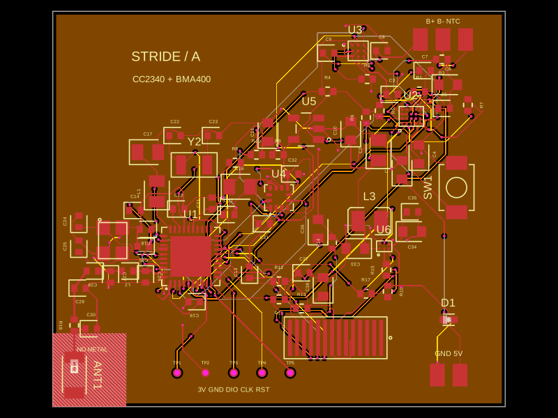
This code defines schematic symbols and 3D footprints for various hardware components such as antennas, sensors, regulators, and connectors used in electronic circuit design.
- Version
- 1.0.4
- License
- unset
- Stars
- 0
review/FUNCTIONAL-AUDIT.md
PCB
# Pedometer functional review — 2026-09-07

**The architecture matches the requested pedometer, but this project is not ready to order as a working product.** This is a source, connectivity, layout, and datasheet review. No assembled board, programmed firmware, battery-life measurement, or RF test has been performed.

## Match to the requested product

| Requirement | Present in this design | Validation status |
|---|---|---|
| Bluetooth MCU | U1, individual CC2340R5 QFN | Connected; firmware and RF performance unverified |
| Rechargeable battery charger | U2, individual BQ25150 | Connected; exact protected cell, NTC, and charge settings need validation |
| Fuel gauge | U3, individual BQ27427 | Connected in the cell-current path; cell-specific setup required |
| Accelerometer / steps | U4, individual BMA400 | Connected over I²C with both interrupts; step-count firmware required |
| Small display | DS1, bare 0.91-inch OLED glass and flex | Flex solder lands present; glass is a hand-installed item |
| Weeks of battery life | Assumed 100 mAh protected LiPo, brief screen use | Budget only; not measured |
| Chip-level construction | ICs, passives, antenna, crystals, and bare glass | No breakout or radio modules |

The PCB is 40 × 35 mm, four layers, 0.8 mm thick. Those dimensions and the 100 mAh cell are design assumptions, not a completed enclosure or battery selection.

## Findings to resolve before ordering

1. **U6's imported footprint needs correction or explicit assembler acceptance.** `imports/TPS61046YFFR.tsx` defines six pads with radius 0.0919988 mm, giving a diameter of **0.1839976 mm**. TI's YFF0006 example land pattern shows **0.23 mm** exposed lands. JLCPCB publishes a **0.20 mm** minimum BGA pad diameter. The current import is smaller than that published minimum. Verify the ball map, copper, mask, paste apertures, and placement rotation together after correcting it. This footprint has not been changed in the shorts repair. [TI package drawing, page 24](https://www.ti.com/lit/ds/symlink/tps61046.pdf), [JLCPCB capabilities](https://jlcpcb.com/capabilities/pcb-capabilities).

2. **RF, crystals, and switching-power layout still require engineering review.** The provisional 0.18 mm RF width has not been calculated against a selected stackup. Oscillator routes and switching-node routes also need review against their manufacturers' reference layouts. Check the antenna feed, ground continuity, matching components, oscillator loop lengths, decoupling, and boost current loops before fabrication. Final antenna tuning must include the battery and enclosure. Routing DRC does not verify these analog requirements. Measurements from the regenerated copper are recorded in `critical-route-metrics.json`. [TI CC2340R5 reference](https://www.ti.com/lit/ds/symlink/cc2340r5.pdf), [Johanson antenna guidance](https://www.johansontechnology.com/datasheets/2450AT18A100/2450AT18A100.pdf).

3. **The display supply needs a tolerance and sequencing check.** The 82 kΩ / 10 kΩ divider produces a nominal 7.314 V. Using 1% resistor extremes and the regulator's 0.811 V maximum PWM reference gives approximately **7.595 V**, before ripple and feedback-current effects. The OLED external-VCC application drawing specifies 7–7.5 V, although its DC table allows 6.4–9.0 V. This is an application-target margin issue, not evidence that the display will certainly fail. Resolve that specification difference, select the divider accordingly, and measure startup, light-load ripple, and shutdown sequencing. [TI electrical characteristics](https://www.ti.com/lit/ds/symlink/tps61046.pdf), [OLED specification, pages 8 and 11–12](https://datasheet.lcsc.com/datasheet/pdf/293805b83cbd2adf5057f47431bcbc3e.pdf?productCode=C18723017).

4. **The selected manufacturing process has not been validated against all copper geometry.** The board uses 0.15 mm via holes / 0.25 mm pads and permits automatic via-in-pad. Filled and copper-capped vias, appropriate surface finish, stencil design, and assembly inspection need to match the actual fine-pitch lands. The project's 0.09 mm routing clearance checks do not establish compliance with every drill-to-copper rule in the fabricator's capabilities. Perform DFM on the final Gerbers and drill stack. [JLCPCB capabilities](https://jlcpcb.com/capabilities/pcb-capabilities).

## Why ordering alone will not produce a working pedometer

`docs/firmware-and-interfaces.md` is an integration specification. There is **no flashable MCU application** in this project. Firmware must initialize the sensor, count and preserve steps, drive the display, expose BLE services, configure the gauge and charger, and enter low-power states. A blank MCU will not perform those tasks. A generic BLE inspection app can test initial firmware; a dedicated phone app is optional for that bench test.

DS1 is marked `doNotPlace` and appears as **HAND INSTALL** in the review BOM. Automated PCBA population excludes the glass. The protected battery, thermistor, charging dock, programming probe, display support, and enclosure must also be supplied or assembled separately. Check the real folded flex and battery clearance while keeping the antenna corner clear of metal.

The power connections support the intended architecture: the gauge's BAT-to-SRX current path separates PACK_P from BAT_SYS; the charger supplies PMID; an always-on regulator supplies 3 V to the MCU and sensor. The OLED has separately controlled logic and high-voltage supplies. Charger CE is pulled high so firmware can configure charging before enabling it. These observations establish the intended topology, not measured startup or charging behavior.

The shared I²C bus addresses are documented for the accelerometer, charger, and gauge. The OLED uses separate GPIOs and a software I²C bus. The BMA400 hardware step counter must be enabled and configured for wrist or pocket use; its presence does not validate real-world step accuracy. [Bosch BMA400 datasheet](https://www.bosch-sensortec.com/media/boschsensortec/downloads/datasheets/bst-bma400-ds000.pdf).

## Battery-life acceptance

The current budget assumes 80 mAh usable from a 100 mAh cell. Four weeks requires average battery current at or below **119 µA**. The example budget is 79.7 µA, approximately 42 days, with only 100 seconds of display use per day and infrequent BLE activity. A continuous 30 mA display load would use the same capacity in about 2.7 hours. These are arithmetic estimates, not board measurements.

After the design issues are resolved, program and bench-test a small prototype batch. Measure rail startup, charger/NTC behavior, display sequencing, step accuracy, sleep and radio current, and BLE range. Only those results can establish whether the finished assembly meets the requested weeks-long runtime and pedometer behavior. The detailed bring-up sequence is in `docs/design.md`.

## Measured routing observations

These are planar lengths in the final generated copper; via depth is excluded. They are review inputs, not acceptance thresholds.

| Connection | Length | Layers | Via transitions |
|---|---:|---|---:|
| U6.SW → L3.pin2 | 4.920 mm | inner2, top | 2 |
| U1.DIO4_X32N → Y2.pin2 | 7.931 mm | inner1, top | 2 |
| U1.DIO3_X32P → Y2.pin1 | 9.787 mm | inner2, top | 2 |
| U1.X48N → Y1.X2 | 3.901 mm | top | 0 |
| U1.X48P → Y1.X1 | 6.804 mm | bottom, top | 2 |

The long oscillator loops and switching-node layer changes need attention before fabrication. Compare these paths and their returns to the manufacturers’ layouts. Ground pours may provide additional return paths beyond individual ground traces.