MustafaMulla29/stride-pedometer
This code defines schematic symbols and 3D footprints for various hardware components such as antennas, sensors, regulators, and connectors used in electronic circuit design.
- Version
- 1.0.4
- License
- unset
- Stars
- 0
imports/DFE201610E_100M_P2.tsx
import type { ChipProps } from "@tscircuit/props"

const pinLabels = {
  pin1: ["pin1"],
  pin2: ["pin2"]
} as const

export const DFE201610E_100M_P2 = (props: ChipProps<typeof pinLabels>) => {
  return (
    <chip
      pinLabels={pinLabels}
      symbol={
        <symbol>
          <port name="pin2" pinNumber={2} aliases={["2"]} direction="right" schX={0.4} schY={0} schStemLength={0.06} />
          <port name="pin1" pinNumber={1} aliases={["1"]} direction="left" schX={-0.4} schY={0} schStemLength={0.06} />
          <schematicpath svgPath="M -0.3376 0.0014 A 0.08 0.078 0 1 0 -0.1784 0.0012" strokeColor="#880000" />
          <schematicpath svgPath="M -0.168 0.0014 A 0.08 0.078 0 1 0 -0.0088 0.0014" strokeColor="#880000" />
          <schematicpath svgPath="M 0.0014 0.0014 A 0.08 0.078 0 1 0 0.1606 0.0014" strokeColor="#880000" />
          <schematicpath svgPath="M 0.174 0.0014 A 0.08 0.078 0 1 0 0.3334 0.0012" strokeColor="#880000" />
        </symbol>
      }
      supplierPartNumbers={{
  "jlcpcb": [
    "C426327"
  ]
}}
      manufacturerPartNumber="DFE201610E-100M=P2"
      footprint={<footprint>
        <smtpad portHints={["pin2"]} pcbX="0.999998mm" pcbY="0mm" width="1.1999976mm" height="1.7999964mm" shape="rect" />
<smtpad portHints={["pin1"]} pcbX="-0.999998mm" pcbY="0mm" width="1.1999976mm" height="1.7999964mm" shape="rect" />
<silkscreenpath route={[{"x":-0.4999990000000025,"y":1.1999975999999606},{"x":-1.54998420000004,"y":1.1999975999999606}]} />
<silkscreenpath route={[{"x":-0.4999990000000025,"y":-1.1999976000000743},{"x":-1.54998420000004,"y":-1.1999976000000743}]} />
<silkscreenpath route={[{"x":0.49999899999988884,"y":1.1999975999999606},{"x":1.54998420000004,"y":1.1999975999999606}]} />
<silkscreenpath route={[{"x":0.49999899999988884,"y":-1.1999976000000743},{"x":1.54998420000004,"y":-1.1999976000000743}]} />
<silkscreenpath route={[{"x":-1.8999708000001192,"y":0.9999979999998914},{"x":-1.8999708000001192,"y":-0.9999979999998914}]} />
<silkscreenpath route={[{"x":1.8999708000000055,"y":0.9999979999998914},{"x":1.8999708000000055,"y":-0.9999979999998914}]} />
<silkscreenpath route={[{"x":-1.54998420000004,"y":1.1999975999999606},{"x":-1.6999712000001637,"y":1.1999975999999606},{"x":-1.8999708000001192,"y":0.9999979999998914}]} />
<silkscreenpath route={[{"x":-1.54998420000004,"y":-1.1999976000000743},{"x":-1.6999712000001637,"y":-1.1999976000000743},{"x":-1.8999708000001192,"y":-0.9999979999998914}]} />
<silkscreenpath route={[{"x":1.54998420000004,"y":1.1999975999999606},{"x":1.6999711999999363,"y":1.1999975999999606},{"x":1.8999708000000055,"y":0.9999979999998914}]} />
<silkscreenpath route={[{"x":1.54998420000004,"y":-1.1999976000000743},{"x":1.6999711999999363,"y":-1.1999976000000743},{"x":1.8999708000000055,"y":-0.9999979999998914}]} />
<silkscreentext text="{NAME}" pcbX="0.009398mm" pcbY="2.1938mm" anchorAlignment="center" fontSize="1mm" />
<courtyardoutline outline={[{"x":-2.1456020000000535,"y":1.4437999999998965},{"x":2.164397999999892,"y":1.4437999999998965},{"x":2.164397999999892,"y":-1.4438000000001239},{"x":-2.1456020000000535,"y":-1.4438000000001239},{"x":-2.1456020000000535,"y":1.4437999999998965}]} />
      </footprint>}
      cadModel={{
        objUrl: "https://modelcdn.tscircuit.com/easyeda_models/assets/C426327.obj?uuid=969fb22dc7094eac9379f530d4c94913",
        stepUrl: "https://modelcdn.tscircuit.com/easyeda_models/assets/C426327.step?uuid=969fb22dc7094eac9379f530d4c94913",
        pcbRotationOffset: 0,
        modelOriginPosition: { x: 0, y: 0, z: -0.475 },
      }}
      {...props}
    />
  )
}
Related Packages
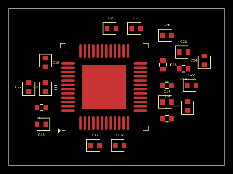 More from this authorMustafaMulla29/ti-chipThis code models a hardware circuit for a motor driver using a DRV83053QPHPQ1 integrated circuit, with power supply bypass capacitors, charge-pump capacitors, resistors, and filters, representing the physical connections and key components in a motor control power stage.
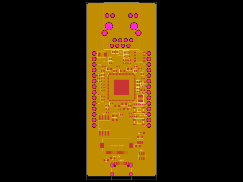 Similar packagemohan-bee/RV1106G2This code defines a detailed hardware schematic with schematic symbols, footprints, and 3D models for various electronic components including microcontrollers, voltage regulators, connectors, and passive parts, designed for PCB layout and routing.
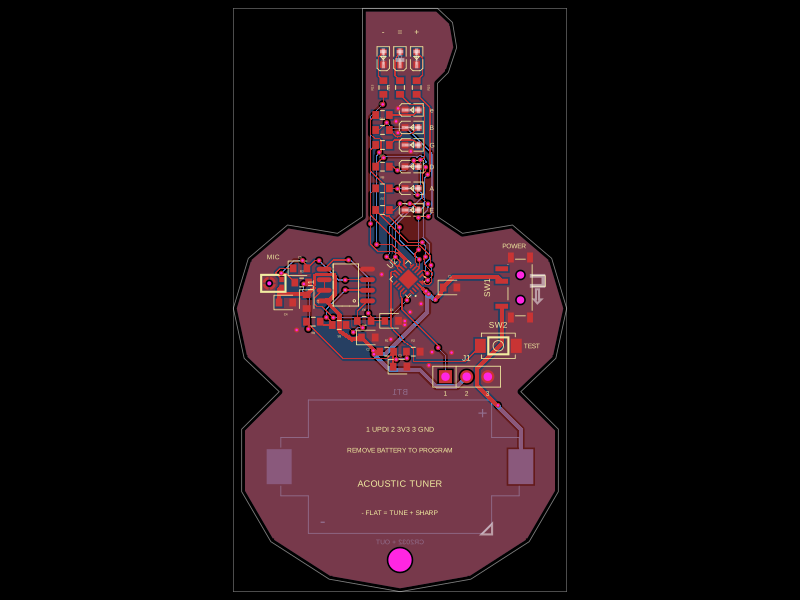 Discover something newgokul/acoustic-guitar-tunerThis code defines the physical pin configuration and footprint layouts for the ATtiny1616 microcontroller and a matching tactile switch component, including their key hardware connection points, dimensions, and 3D models.