MrPicklePinosaur/tscircuit_demo
This circuit hardware provides a USB-to-multi-protocol (I2C/SPI/UART) bridge using an FT232H chip, powered via a 3.3V regulator, with USB-C input, ESD protection, status LEDs, a STEMMA QT connector, and various support components.
Usage: To use this component in a project: 1. Import the specific component: ```tsx import { AMS1117_3_3 } from "@tsci/MrPicklePinosaur.tscircuit_demo/imports/AMS1117_3_3" ``` 2. Use the component in a board layout: ```tsx <board> <AMS1117_3_3 name="U2" /> </board> ``` Key details: - The component has predefined pin labels: - pin1: GND - pin2: VOUT1 - pin3: VIN - pin4: VOUT2 - Supports common layout props - Has a specific SMT footprint - Includes JLCPCB supplier part number (C6186)
- Version
- 1.0.0
- License
- unset
- Stars
- 0
index.tsx
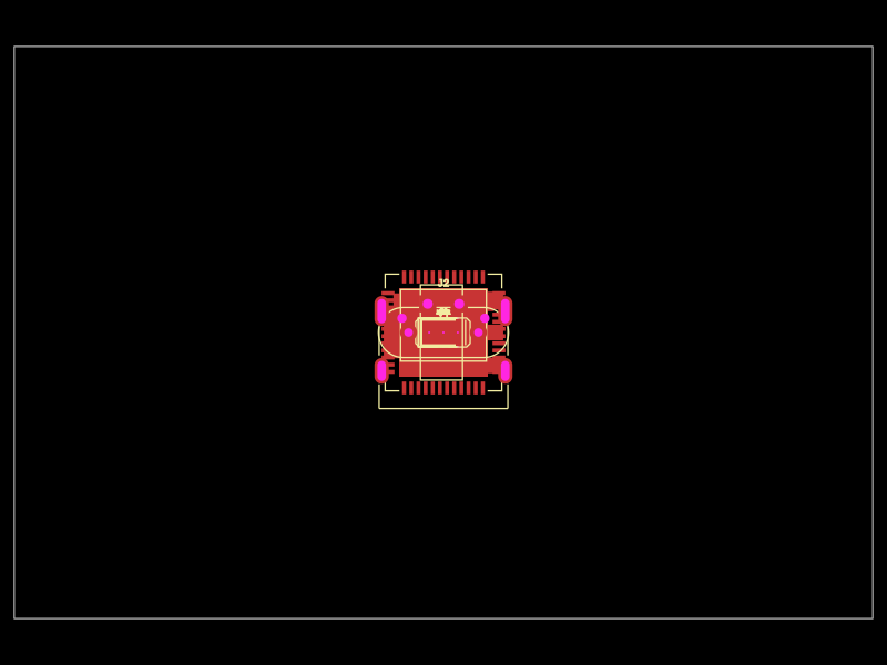
PCB
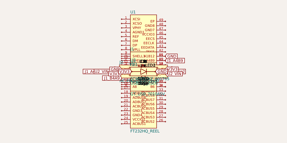
Schematic
/**
 * FT232H USB-to-Multi-Protocol Carrier Board
 *
 * Features:
 * - FTDI FT232H USB bridge (QFN-48 package)
 * - USB-C input (UFP device mode)
 * - 3.3V regulated power rail
 * - STEMMA QT connector (shared I2C/SPI/UART - software configurable)
 * - GPIO header for additional FT232H pins
 * - ESD protection on USB
 * - Status LEDs
 * - Test points for debugging
 *
 * IMPORTANT: FT232H can only operate in ONE mode at a time:
 * - I2C mode: SCL=ADBUS0, SDA=ADBUS1+ADBUS2 (needs external pull-ups)
 * - SPI mode: SCK=ADBUS0, MOSI=ADBUS1, MISO=ADBUS2, CS=ADBUS3+
 * - UART mode: TX=ADBUS0, RX=ADBUS1
 */

import { FT232HQ_REEL } from "./imports/FT232HQ_REEL"
import { GT_USB_7010ASV } from "./imports/GT_USB_7010ASV"
import { AMS1117_3_3 } from "./imports/AMS1117_3_3"
import { USBLC6_2SC6 } from "./imports/USBLC6_2SC6"
import { FCM2012KF_601T05 } from "./imports/FCM2012KF_601T05"

export default () => {
  return (
    <board width="60mm" height="40mm">
      {/* FT232H Main USB Bridge IC - QFN-48 Package */}
      <FT232HQ_REEL name="U1" />

      {/* USB-C Connector (Device/UFP mode) */}
      <GT_USB_7010ASV name="J1" />

      {/* 3.3V LDO Voltage Regulator */}
      <AMS1117_3_3 name="U2" />

      {/* USB ESD Protection */}
      <USBLC6_2SC6 name="U3" />

      {/* STEMMA QT Connector (JST SH 4-pin, 1mm pitch) */}
      {/* This connector shares the same FT232H pins for all modes */}
      <chip
        name="J2"
        manufacturerPartNumber="HC-FPC-1.0-4P-FH20"
        supplierPartNumbers={{ jlcpcb: ["C49166830"] }}
        footprint="jst_sh_4pin_1mm"
        pinLabels={{
          pin1: "GND",
          pin2: "V3V3",
          pin3: "SDA_MOSI_TX",
          pin4: "SCL_SCLK_RX",
        }}
        schPinArrangement={{
          leftSide: {
            direction: "top-to-bottom",
            pins: ["GND", "V3V3"]
          },
          rightSide: {
            direction: "top-to-bottom",
            pins: ["SDA_MOSI_TX", "SCL_SCLK_RX"]
          }
        }}
      />

      {/* 12MHz Crystal for FT232H */}
      <chip
        name="Y1"
        footprint="hc49"
        pinLabels={{
          pin1: "X1",
          pin2: "X2"
        }}
      />

      {/* Bulk capacitors for USB power input */}
      <capacitor
        name="C1"
        capacitance="10uF"
        maxVoltageRating="16V"
        footprint="0805"
      />

      <capacitor
        name="C2"
        capacitance="10uF"
        maxVoltageRating="16V"
        footprint="0805"
      />

      {/* Regulator input/output capacitors */}
      <capacitor
        name="C3"
        capacitance="10uF"
        maxVoltageRating="16V"
        footprint="0805"
      />

      <capacitor
        name="C4"
        capacitance="10uF"
        maxVoltageRating="6.3V"
        footprint="0805"
      />

      {/* FT232H VCC decoupling (3.3V core) */}
      <capacitor
        name="C5"
        capacitance="100nF"
        footprint="0603"
      />

      <capacitor
        name="C6"
        capacitance="100nF"
        footprint="0603"
      />

      <capacitor
        name="C7"
        capacitance="4.7uF"
        maxVoltageRating="6.3V"
        footprint="0603"
      />

      {/* FT232H VCCIO decoupling (3.3V I/O) */}
      <capacitor
        name="C8"
        capacitance="100nF"
        footprint="0603"
      />

      <capacitor
        name="C9"
        capacitance="100nF"
        footprint="0603"
      />

      <capacitor
        name="C10"
        capacitance="100nF"
        footprint="0603"
      />

      <capacitor
        name="C11"
        capacitance="100nF"
        footprint="0603"
      />

      {/* FT232H REF pin capacitor */}
      <capacitor
        name="C12"
        capacitance="100nF"
        footprint="0603"
      />

      {/* Crystal load capacitors */}
      <capacitor
        name="C13"
        capacitance="27pF"
        footprint="0603"
      />

      <capacitor
        name="C14"
        capacitance="27pF"
        footprint="0603"
      />

      {/* USB-C CC pulldown resistors (5.1k for UFP device mode) */}
      <resistor
        name="R1"
        resistance="5.1k"
        footprint="0603"
      />

      <resistor
        name="R2"
        resistance="5.1k"
        footprint="0603"
      />

      {/* FT232H RESET# pull-up resistor */}
      <resistor
        name="R3"
        resistance="10k"
        footprint="0603"
      />

      {/* I2C pull-up resistors (4.7k typical for 3.3V I2C) */}
      {/* Optional - can be populated for I2C mode */}
      <resistor
        name="R4"
        resistance="4.7k"
        footprint="0603"
      />

      <resistor
        name="R5"
        resistance="4.7k"
        footprint="0603"
      />

      {/* LED current limiting resistors */}
      <resistor
        name="R6"
        resistance="1k"
        footprint="0603"
      />

      <resistor
        name="R7"
        resistance="1k"
        footprint="0603"
      />

      {/* Ferrite bead for power supply filtering */}
      <FCM2012KF_601T05 name="FB1" />

      {/* Status LEDs - Bi-color (Red/Green) */}
      <led
        name="LED1"
        color="green"
        footprint="0603"
      />

      <led
        name="LED2"
        color="red"
        footprint="0603"
      />

      {/* === POWER CONNECTIONS === */}

      {/* USB-C VBUS to ferrite bead */}
      <trace from="J1.B4A9" to="FB1.pin1" />
      <trace from="J1.A4B9" to="FB1.pin1" />

      {/* Ferrite bead to bulk capacitor and regulator input */}
      <trace from="FB1.pin2" to="C1.pin1" />
      <trace from="C1.pin1" to="U2.VIN" />
      <trace from="C1.pin1" to="C3.pin1" />

      {/* USB-C GND connections */}
      <trace from="J1.B1A12" to="net.GND" />
      <trace from="J1.A1B12" to="net.GND" />
      <trace from="C1.pin2" to="net.GND" />
      <trace from="C3.pin2" to="net.GND" />
      <trace from="U2.GND" to="net.GND" />

      {/* Regulator output to 3.3V net */}
      <trace from="U2.VOUT1" to="net.V3V3" />
      <trace from="U2.VOUT2" to="net.V3V3" />
      <trace from="C4.pin1" to="net.V3V3" />
      <trace from="C2.pin1" to="net.V3V3" />
      <trace from="C2.pin2" to="net.GND" />
      <trace from="C4.pin2" to="net.GND" />

      {/* === USB DATA CONNECTIONS === */}

      {/* USB-C CC pulldowns for UFP device mode */}
      <trace from="J1.A5" to="R1.pin1" />
      <trace from="R1.pin2" to="net.GND" />
      <trace from="J1.B5" to="R2.pin1" />
      <trace from="R2.pin2" to="net.GND" />

      {/* USB D+/D- through ESD protection to FT232H */}
      <trace from="J1.A6" to="U3.pin3" />  {/* D+ */}
      <trace from="J1.A7" to="U3.pin1" />  {/* D- */}
      <trace from="U3.pin2" to="net.GND" />
      <trace from="U3.pin5" to="net.V3V3" />
      <trace from="U3.pin4" to="U1.pin6" />  {/* D+ output to FT232H */}
      <trace from="U3.pin6" to="U1.pin7" />  {/* D- output to FT232H */}

      {/* === FT232H POWER CONNECTIONS === */}

      {/* FT232H USB power input from filtered VBUS */}
      <trace from="FB1.pin2" to="U1.pin40" />  {/* VREGIN */}

      {/* FT232H 3.3V core supply (VCC) with decoupling */}
      <trace from="net.V3V3" to="U1.pin38" />  {/* VCCCORE */}
      <trace from="U1.pin38" to="C5.pin1" />
      <trace from="C5.pin2" to="net.GND" />
      <trace from="C6.pin1" to="net.V3V3" />
      <trace from="C6.pin2" to="net.GND" />
      <trace from="C7.pin1" to="net.V3V3" />
      <trace from="C7.pin2" to="net.GND" />

      {/* FT232H 3.3V I/O supply (VCCIO) with decoupling */}
      <trace from="net.V3V3" to="U1.pin12" />  {/* VCCIO1 */}
      <trace from="net.V3V3" to="U1.pin24" />  {/* VCCIO2 */}
      <trace from="net.V3V3" to="U1.pin46" />  {/* VCCIO3 */}
      <trace from="net.V3V3" to="U1.pin3" />   {/* VPHY */}
      <trace from="net.V3V3" to="U1.pin8" />   {/* VPLL */}
      <trace from="net.V3V3" to="U1.pin37" />  {/* VCCA */}
      <trace from="net.V3V3" to="U1.pin39" />  {/* VCCD */}
      <trace from="C8.pin1" to="net.V3V3" />
      <trace from="C8.pin2" to="net.GND" />
      <trace from="C9.pin1" to="net.V3V3" />
      <trace from="C9.pin2" to="net.GND" />
      <trace from="C10.pin1" to="net.V3V3" />
      <trace from="C10.pin2" to="net.GND" />
      <trace from="C11.pin1" to="net.V3V3" />
      <trace from="C11.pin2" to="net.GND" />

      {/* FT232H ground connections */}
      <trace from="U1.pin10" to="net.GND" />  {/* GND1 */}
      <trace from="U1.pin11" to="net.GND" />  {/* GND2 */}
      <trace from="U1.pin22" to="net.GND" />  {/* GND3 */}
      <trace from="U1.pin23" to="net.GND" />  {/* GND4 */}
      <trace from="U1.pin35" to="net.GND" />  {/* GND5 */}
      <trace from="U1.pin36" to="net.GND" />  {/* GND6 */}
      <trace from="U1.pin47" to="net.GND" />  {/* GND7 */}
      <trace from="U1.pin48" to="net.GND" />  {/* GND8 */}
      <trace from="U1.pin49" to="net.GND" />  {/* EP (exposed pad) */}
      <trace from="U1.pin4" to="net.GND" />   {/* AGND1 */}
      <trace from="U1.pin9" to="net.GND" />   {/* AGND2 */}
      <trace from="U1.pin41" to="net.GND" />  {/* AGND3 */}

      {/* FT232H REF pin capacitor */}
      <trace from="U1.pin5" to="C12.pin1" />  {/* REF */}
      <trace from="C12.pin2" to="net.GND" />

      {/* === FT232H CONFIGURATION === */}

      {/* RESET# pull-up - Note: FT232H doesn't have RESET# pin, using PWREN# instead */}
      {/* <trace from="U1.RESET#" to="R3.pin1" /> */}
      {/* <trace from="R3.pin2" to="net.V3V3" /> */}

      {/* TEST pin to ground */}
      <trace from="U1.pin42" to="net.GND" />  {/* TEST */}

      {/* Crystal oscillator */}
      <trace from="U1.pin1" to="Y1.X1" />  {/* XCSI (crystal input) */}
      <trace from="U1.pin2" to="Y1.X2" />  {/* XCSO (crystal output) */}
      <trace from="Y1.X1" to="C13.pin1" />
      <trace from="C13.pin2" to="net.GND" />
      <trace from="Y1.X2" to="C14.pin1" />
      <trace from="C14.pin2" to="net.GND" />

      {/* === STEMMA QT CONNECTOR === */}

      {/* Power to STEMMA QT */}
      <trace from="J2.V3V3" to="net.V3V3" />
      <trace from="J2.GND" to="net.GND" />

      {/* Multi-protocol data lines (I2C/SPI/UART shared) */}
      <trace from="J2.SCL_SCLK_RX" to="U1.pin13" />  {/* ADBUS0 */}
      <trace from="J2.SDA_MOSI_TX" to="U1.pin14" />  {/* ADBUS1 */}

      {/* Optional I2C pull-ups (can be populated for I2C mode) */}
      <trace from="R4.pin1" to="net.V3V3" />
      <trace from="R4.pin2" to="U1.pin13" />  {/* ADBUS0 */}
      <trace from="R5.pin1" to="net.V3V3" />
      <trace from="R5.pin2" to="U1.pin14" />  {/* ADBUS1 */}

      {/* === STATUS LEDS === */}

      {/* Power LED (Green) */}
      <trace from="net.V3V3" to="R6.pin1" />
      <trace from="R6.pin2" to="LED1.pin1" />
      <trace from="LED1.pin2" to="net.GND" />

      {/* Activity LED (Red) - Note: FT232H doesn't have PWREN# in pinLabels, skipping for now */}
      {/* <trace from="U1.PWREN#" to="R7.pin1" /> */}
      <trace from="R7.pin2" to="LED2.pin1" />
      <trace from="LED2.pin2" to="net.GND" />

      {/* === GPIO HEADER === */}
      {/* 2.54mm pin header for additional GPIO and SPI signals */}
      <pinheader
        name="J3"
        pinCount={16}
        pitch="2.54mm"
        gender="male"
        pinLabels={[
          "GND",
          "3V3",
          "ADBUS2_MISO",
          "ADBUS3_CS",
          "ADBUS4",
          "ADBUS5",
          "ADBUS6",
          "ADBUS7",
          "ACBUS0",
          "ACBUS1",
          "ACBUS2",
          "ACBUS3",
          "ACBUS4",
          "ACBUS5",
          "ACBUS6",
          "ACBUS7",
        ]}
      />

      {/* GPIO header connections */}
      <trace from="J3.GND" to="net.GND" />
      <trace from="J3.3V3" to="net.V3V3" />
      <trace from="J3.ADBUS2_MISO" to="U1.pin15" />  {/* ADBUS2 */}
      <trace from="J3.ADBUS3_CS" to="U1.pin16" />    {/* ADBUS3 */}
      <trace from="J3.ADBUS4" to="U1.pin17" />       {/* ADBUS4 */}
      <trace from="J3.ADBUS5" to="U1.pin18" />       {/* ADBUS5 */}
      <trace from="J3.ADBUS6" to="U1.pin19" />       {/* ADBUS6 */}
      <trace from="J3.ADBUS7" to="U1.pin20" />       {/* ADBUS7 */}
      <trace from="J3.ACBUS0" to="U1.pin21" />       {/* ACBUS0 */}
      <trace from="J3.ACBUS1" to="U1.pin25" />       {/* ACBUS1 */}
      <trace from="J3.ACBUS2" to="U1.pin26" />       {/* ACBUS2 */}
      <trace from="J3.ACBUS3" to="U1.pin27" />       {/* ACBUS3 */}
      <trace from="J3.ACBUS4" to="U1.pin28" />       {/* ACBUS4 */}
      <trace from="J3.ACBUS5" to="U1.pin29" />       {/* ACBUS5 */}
      <trace from="J3.ACBUS6" to="U1.pin30" />       {/* ACBUS6 */}
      <trace from="J3.ACBUS7" to="U1.pin31" />       {/* ACBUS7 */}

      {/* === TEST POINTS === */}
      {/* Add test points for critical signals */}
      <testpoint name="TP1" footprintVariant="pad" padShape="circle" padDiameter="1mm" />
      <testpoint name="TP2" footprintVariant="pad" padShape="circle" padDiameter="1mm" />
      <testpoint name="TP3" footprintVariant="pad" padShape="circle" padDiameter="1mm" />
      <testpoint name="TP4" footprintVariant="pad" padShape="circle" padDiameter="1mm" />
      <testpoint name="TP5" footprintVariant="pad" padShape="circle" padDiameter="1mm" />
      <testpoint name="TP6" footprintVariant="pad" padShape="circle" padDiameter="1mm" />

      {/* Test point connections for debugging */}
      <trace from="TP1.tp" to="net.V3V3" />
      <trace from="TP2.tp" to="net.GND" />
      <trace from="TP3.tp" to="U1.pin13" />  {/* ADBUS0 */}
      <trace from="TP4.tp" to="U1.pin14" />  {/* ADBUS1 */}
      <trace from="TP5.tp" to="U1.pin7" />   {/* DP (USB D+) */}
      <trace from="TP6.tp" to="U1.pin6" />   {/* DM (USB D-) */}

  </board>
)
}