Devesh36/pocket-audio-player
A portable, rechargeable microSD audio player built around an RP2040, SPI flash, USB‑C charging/power management, LCD/button controls, PCM5102A I²S DAC, and TPA6132A headphone amplifier in a 3D‑printed enclosure.
- Version
- 1.0.12
- License
- unset
- Stars
- 0
README.md
# Pocket audio player — reference-style assembly

A portable microSD stereo-player hardware prototype authored entirely in **tscircuit TypeScript/TSX**. The assembly follows the supplied early iPod reference: a white rounded front, silver back/rim, landscape 1.9-inch menu screen, four circular quadrant buttons and a center select button. A protected rechargeable battery sits below the lower half of the PCB.

The screen menu is a static 3D preview. Playback/menu firmware and physical fit testing are still required. The display is now a specified Waveshare module with its matching SPI interface. The circular inner face is stationary: this revision provides five tactile actions, without a rotary encoder or touch-scroll sensor. The exterior is reference-matched; it is not an exact dimensional reproduction of an Apple device.

## PCB and power

- 60 × 90 mm, four layers, 1.6 mm PCB with four 2.7 mm mounting holes.
- RP2040, 2 MB QSPI flash, 12 MHz crystal, SPI microSD, PCM5102A stereo DAC and TPA6132A2 headphone amplifier.
- USB-C supplies 5 V for charging and RP2040 USB programming. Separate 5.1 kΩ CC resistors and USBLC6-2SC6 protect the data interface.
- MCP73831-2 single-cell 4.2 V charger, R_PROG=10 kΩ, approximately **100 mA** charge current. AO3401A/SS14 load sharing and TPS63031 provide the system's regulated 3.3 V.
- The modeled battery uses the published **29 × 36 × 4.75 mm** envelope of [Adafruit 1578](https://www.adafruit.com/product/1578), a protected 3.7 V / 500 mAh LiPo. Its specified charging limit is 500 mA, above this board's 100 mA setting. No runtime measurement is claimed.
- AUX is a 3.5 mm stereo headphone output. The signal path has a 1:2 divider followed by a −6 dB amplifier setting; start firmware with low digital volume.

The battery is located at X=0 / Y=−29 / Z=−3.5, underneath the controls and PCB. A locating tray and 0.6 mm insulating adhesive pad retain it without a hard pouch clamp. Its JST-PH plug mates directly with **J_BAT, JST B2B-PH-K-S, 2 mm pitch**. Pin 1 is GND and pin 2 is positive VBAT, matching Adafruit's PH battery connection. Check a replacement cell's polarity before plugging it in. Red/black lead CAD is illustrative.

The charging path is **USB-C VBUS → MCP73831-2 → VBAT → J_BAT pin 2 → protected cell**; J_BAT pin 1 returns to GND. USB 5 V does not connect directly to the cell. The cell also feeds the load-sharing circuit and ADC divider. Charging remains available with J_PWR open. The existing 100 mA charge setting is retained.

## Case and controls

`index.circuit.tsx` combines the board, `<assembly.printedpart>` case/button geometry, `<assembly.screen>` LCD and `<assembly.subassembly>` battery models. The case, buttons and battery geometry use tscircuit JSCAD elements. The display uses Waveshare manufacturer CAD imported into a native tscircuit CAD plan, with a static menu overlay.

- Body: **64 × 110 × 18.1 mm**, 1.0 mm floor and 1.2 mm front, rounded corners, white front and silver back/rim. Controls protrude 0.9 mm above the front.
- The 54 mm circular control ring has menu at the top, previous at the left, next at the right and play/pause at the bottom, surrounding a 15 mm center select button. Four independently moving sectors use lever arms to reach the existing switches. Diagonal ribs support the fixed inner face and clear the moving sectors.
- Each actuator has a nominal 0.25 mm rest gap above its switch. Travel, feel and retention require a printed prototype; these are not qualified switch mechanisms.
- Four posts align with X ±26 / Y ±41. Use M2.5 plastic tapping screws with at most 3.7 mm engagement in the 2 mm pilots; verify head clearance on the populated board.
- A locating lip has 0.3 mm clearance per side. Four pairs of 3 × 1 mm disc magnets retain the front; pockets are 3.2 mm diameter × 1.1 mm deep. Match magnet polarities before gluing.
- Top-edge recesses expose USB-C and AUX; a left-side opening exposes microSD. BOOT, RESET and the power shunt are accessible after removing the front, keeping the visible face close to the reference.
- `enclosure-preview.circuit.tsx` lifts the front/screen/buttons 35 mm, drops the back 28 mm and moves the battery aside for inspection. These offsets are visualization only.

The screen and battery connectors, display signals and ADC pin assignment have changed. The PCB is rerouted for Rev B. Switch net names/silkscreen still use the original play/volume labels; firmware should apply the assembly mapping below.

## Screen

The selected screen is the [Waveshare 1.9inch LCD Module](https://www.waveshare.com/1.9inch-lcd-module.htm): **ST7789V2 IPS, 170 × 320 pixels**, used in landscape as **320 × 170**. The module is **51.2 × 27.3 mm**, with a **42.72 × 22.70 mm** active area. A **43.72 × 23.7 mm** front opening at X=0 / Y=17.2 matches that area. The real manufacturer model places its PCB at Z=6.5–8.1 mm and glass face at Z=10.0 mm, recessed below the 10.6 mm front. The screen stays centered horizontally and sits lower to clear the AUX body and its mounting stud. Four M2 mount points are X ±22.8 / Y 6.35 and 28.05; short fasteners and mount engagement require prototype verification.

**J_LCD** is [JST BM08B-GHS-TBT(LF)(SN)](https://www.jst.com/wp-content/uploads/2021/08/eGH-new.pdf), an eight-contact **1.25 mm GH** top-entry socket, imported with the official tscircuit CLI (`C133062`). It sits at X=0 / Y=−7, below the LCD footprint, so its **7.3 mm mated height** does not collide with the display PCB. Use a short GH-to-GH harness with **GHR-08V-S** housings, one-to-one numbered contacts; the manufacturer's supplied GH-to-individual-header cable needs the appropriate second GH end. Verify continuity by contact number; a mirrored/crisscrossed harness is incompatible.

The [manufacturer schematic](https://files.waveshare.com/upload/7/7f/1.9inch_LCD_Module.pdf) numbers its socket **1 BL, 2 RST, 3 D/C, 4 CS, 5 SCL (SPI clock), 6 SDA (SPI MOSI), 7 GND, 8 VCC**. SCL/SDA on this module are SPI signals. Power and MCU logic use **3.3 V**. The module includes its own level shifter, regulator and backlight driver. The former I²C pull-ups are replaced by 100 kΩ CS/RST pull-ups, and the connector has 100 nF + 10 µF decoupling. Its backlight defaults on through the module's internal pull-up; firmware takes control of BL for PWM dimming.

The display uses **SPI1**, independent of the microSD's SPI0. Firmware must initialize ST7789V2 for the 170 × 320 panel and landscape rotation, including the manufacturer's panel offsets. The rendered iPod header, battery icon and song menu are a static preview; live song titles, navigation and battery percentage require firmware.

`oled-shape.tsx` retains its historical filename but contains the actual LCD geometry/menu definition. `lcd-model-plan.json` is generated from the manufacturer STEP, and `oled-model.ts` embeds the native tscircuit GLB. `<assembly.screen connectsTo=".J_LCD">` attaches it to the updated board.

## Connectors and firmware pins

Pin numbers refer to schematic/pad numbering, not viewing direction.

Purchase **J_LCD, BM08B-GHS-TBT(LF)(SN), [LCSC C133062](https://www.lcsc.com/product-detail/C133062.html)** and **J_PWR, PZ254V-11-02P, [LCSC C492401](https://www.lcsc.com/product-detail/C492401.html)** separately and solder them during assembly. Their existing footprints and part numbers are retained. The BOM lists LCSC for these two parts because tscircuit's JLC search index returns no entry for either ID; this does not mean the parts are discontinued. Other supplier selections remain as specified.

- **J_BAT:** 1 GND, 2 VBAT; JST-PH B2B-PH-K-S, matching the protected Adafruit 1578 cell plug.
- **J_PWR:** bridge to enable the regulator, remove to switch off. USB charging remains available; there is no electronic power latch.
- **J_LCD:** 1 BL (GPIO 19/PWM), 2 RST (GPIO 21), 3 D/C (GPIO 20), 4 CS (GPIO 25), 5 CLK (GPIO 26/SPI1 SCK), 6 DIN (GPIO 27/SPI1 TX), 7 GND, 8 3.3 V. The two metal mounting pads are grounded.
- **J_SWD:** 1 3.3 V, 2 SWDIO, 3 SWCLK, 4 GND.
- **J_AUX:** 2 left/tip, 3 right/ring, 4 and 5 GND; no microphone input.
- **Controls:** GPIO 8 center select (SW_PLAY / BTN_PLAY), 9 previous, 10 next, 11 menu (SW_UP / BTN_UP), 12 play/pause (SW_DOWN / BTN_DOWN). Active low; enable MCU pull-ups. Volume can be implemented in a firmware menu.
- **SD:** GPIO 4 MISO, 5 CS, 6 clock, 7 MOSI; GPIO 13 card detect, active low.
- **Audio:** GPIO 14 DAC unmute, 15 amplifier enable; both have pull-downs. Keep them low at startup. GPIO 16 / 17 / 18 are PIO I²S bit clock / word clock / data.
- **Battery sense:** GPIO 28/ADC2, 100 kΩ / 100 kΩ divider; cell voltage is twice the ADC input.

Firmware can stream WAV through PIO I²S. MP3 decoding is not implemented or benchmarked. No firmware or measured playback result is included.

## Native exports and checks

`dist/enclosure/` contains `case-base.stl`, `case-lid.stl`, `button-plunger.stl` and `ring-button.stl`: print one center plunger and **four ring sectors**, plus the two case pieces. STLs sit at Z=0; front/buttons are inverted for printing. Tune supports, adhesive, magnet fit and tolerances on a prototype.

`dimensions.json`, `fit-check.json` and `mesh-check.json` record positive solid volume, closed consistently wound STL edges, one connected mesh per printed part, mounting-hole alignment and zero unintended intersections between the case, PCB envelope, LCD, cell and moving controls. The 49 manufacturer display meshes and conservative battery/display connector envelopes are checked against the case. The display is also checked against the 21 supplied PCB body models; a broad bounding-box check is followed by exact mesh intersection where needed. These checks do not qualify every populated body, cable or fastener. The assembly is not physically tested.

```sh
bun scripts/generate-mechanical-models.tsx
bun scripts/generate-lcd-model.tsx
bun x tsci export lcd-export.circuit.tsx -f glb -o dist/enclosure/oled-model.glb
bun scripts/embed-oled-model.ts
bun run typecheck
bun run build
bun run export:enclosure
bun run check:enclosure
bun scripts/check-lcd-hardware-fit.tsx
bun scripts/check-lcd-pcb-fit.ts
```

The native PCB, schematic, Circuit JSON, 3D renders and fabrication files are under `dist/index/`. `ipod-front.png`, `ipod-perspective.png` and `ipod-side.png` are rendered directly from the tscircuit-exported GLB. The static viewer is `dist/index.html`; serve `dist` over local HTTP to inspect the assembled and exploded views.

The PCB build and TypeScript checks pass with zero PCB error records. The Rev B copper is checked across all four Gerber layers at 40 pixels/mm. The earlier placement command reported five orientation suggestions while geometric DRC had zero errors/warnings. L1 sourcing and L1/J_AUX assembly rotations remain unverified. Review audio noise, USB signal integrity, charging and physical fit before fabrication. See `validation.json` and `BUGS.md` for evidence and tool limitations.

The imported USB, AUX, microSD, battery and display sockets use native `<connector>` elements. AO3401A uses a P-channel enhancement `<mosfet>`, and the USBLC6-2SC6 VBUS reference pin is explicitly marked as requiring power. The schematic has eight printable A4 pages. USB and crystal pages include schematic-only projections of the RP2040 pins, so their local connections remain visible.

## Development and routing

Requires Bun. The local development package pins tool versions. The lean published package depends on tscircuit and uses `alwaysUseLatestTscircuitOnCloud` for the service's bundled runtime. A successful local build does not imply a successful cloud job; release status is recorded separately.

```sh
bun install
bun run dev
bun run export
```

`routing/candidate.json` retains the validated tscircuit routes. `routing/refinement-notes.json` records local drill/copper clearance refinements after the fresh autoroute, including a short 0.12 mm VBUS escape between the USB vias. `board-router.ts` checks the full input signature before reuse. Changing electrical layout requires setting `useSavedRouting=false`, building with the native router, saving the new routes, restoring the guard and resolving all copper diagnostics before running `bun run check:shorts`. A completed solver alone does not establish a valid PCB. The isolated bug repros are intentionally problematic circuits and are excluded from publication/fabrication builds.

## References

- [Waveshare display documentation](https://www.waveshare.com/wiki/1.9inch_LCD_Module) and [manufacturer 3D model](https://files.waveshare.com/upload/9/98/1.9inch_LCD_Module_3D.zip)
- [JST GH connector drawing](https://www.jst.com/wp-content/uploads/2021/08/eGH-new.pdf)
- [RP2040 hardware guide](https://datasheets.raspberrypi.com/rp2040/hardware-design-with-rp2040.pdf)
- [PCM5102A](https://www.ti.com/lit/ds/symlink/pcm5102a.pdf), [TPA6132A2](https://www.ti.com/lit/ds/symlink/tpa6132a2.pdf), [TPS63031](https://www.ti.com/lit/ds/symlink/tps63031.pdf)
- [MCP73831 charger datasheet](https://ww1.microchip.com/downloads/aemDocuments/documents/APID/ProductDocuments/DataSheets/MCP73831-Family-Data-Sheet-DS20001984H.pdf)
- [Protected battery dimensions and ratings](https://www.adafruit.com/product/1578)
- [tscircuit assembly.screen](https://docs.tscircuit.com/elements/assembly-screen), [assembly.subassembly](https://docs.tscircuit.com/elements/assembly-subassembly)
Related Packages
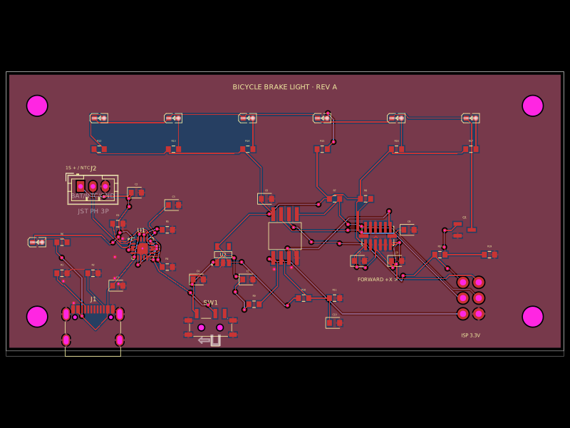 More from this authorDevesh36/bicycle-brake-lightA USB‑C rechargeable 1S Li‑ion bicycle brake-light PCB with BQ24074 charging/protection, 3.3V AVR control, ADXL345 motion sensing, six PWM-driven red LEDs, and ISP programming.
 Similar packageaura/diy-power-delivery-triggerThis hardware design implements a USB Type-C port with supporting power management and signal conditioning components, including a USB-C connector, a FUSB302 USB-C port controller, ESD protection diodes, a buck converter for 3.3V power regulation, an STM32 microcontroller for control and processing, an RGB LED indicator, push button, terminal block connections, and associated filtering and support components.
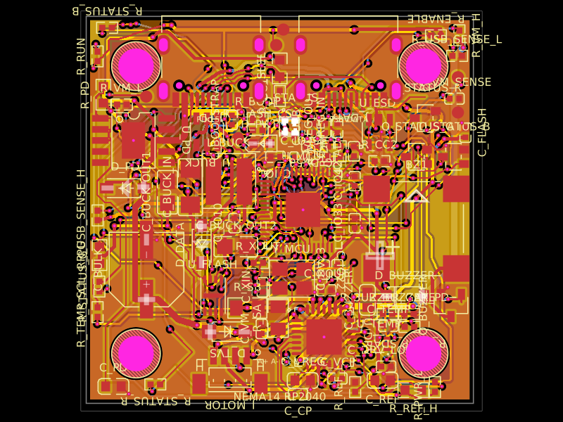 Discover something newAnasSarkiz/NEMA14_RP2040A stepper-motor controller assembly combining an RP2040 board, A4988 driver, buck regulator, MOSFET, and encoder, with a proposed JST-SH harness to a NEMA14 motor.