Devesh36/key-finder
A compact BLE key finder for keys, bags and remotes: replaceable CR2032, piezo alert, status LED and pair button in a 38 mm black keyring enclosure. Includes routed PCB, enclosed/exploded assembly and BOM. Firmware/app and physical qualification remain separate.
- Version
- 0.1.2
- License
- unset
- Stars
- 0
docs/DESIGN.md
# Electrical and mechanical notes

## Power

A replaceable Panasonic CR2032 (20 × 3.2 mm) supplies VBAT directly through the MY-2032-16 holder. ISP1807-LR accepts 1.7–3.6 V at pin 26. C1 is local 100 nF bypass; C2 is 10 µF bulk. There is no regulator quiescent current and no charging circuit. The nRF52840's internal VDD measurement can report battery level without an external divider.

Firmware must use low-duty BLE advertising, sleep, short ringing bursts and a modest TX setting suitable for a coin cell. Loaded battery voltage, ESR, burst current and brownout margin need measurement on fresh and depleted cells. No battery-life or range claim has been verified.

## Pin map

| Function | Module pad | nRF52840 / connection |
| --- | --- | --- |
| Battery | 26 | VCC_nRF / VBAT |
| Ground | 1, 7, 14, 16, 18, 21, 23, 24, 25, 31 | GND |
| Piezo A | 34 | P0.06 → R1 1 kΩ → BZ1.1 |
| Piezo B | 36 | P0.05 → R2 1 kΩ → BZ1.2 |
| Status LED | 32 | P0.08 → R3 3.3 kΩ → LED anode |
| Pair / silence | 38 | P0.03, active low, R4 100 kΩ pull-up |
| Reset | 13 | P0.18 / RESET, R5 100 kΩ pull-up, TP5 |
| SWD data / clock | 28 / 30 | TP3 / TP4 |
| Programmer voltage reference / ground | — | TP1 / TP2 |
| Internal antenna bridge | 20 → 22 | OUT_ANT ↔ OUT_MOD, short top trace |
| USB | 8, 10, 12 | D+, D− and VBUS unused |
| Remaining pins | — | No-connect declarations, including floating mechanical pads |

Drive the two piezo pins with opposite-phase ~4.1 kHz waveforms, then park them at the same level when silent. The disc is capacitive, not an inductive buzzer. Two 1 kΩ series resistors limit a 6 V differential transition to approximately 3 mA; configure GPIO drive strength accordingly. Configure UICR PSELRESET for P0.18 if hardware reset is required. At 3 V supply the ideal differential waveform is 6 Vpp, below the piezo's 30 Vpp maximum. Actual loudness and resonance depend on mounting and need a bench test. This is not a claim of Chipolo's advertised sound level.

## Antenna

DS1807 page 14 requires an **18 mm-wide metal-free region** from the module's midline to the board edge on every PCB layer, except its isolated mechanical pads. U1 is placed at the lower rim; the keyring eye and metal keyring sit at the opposite end. The keepout excludes traces and planes on all four layers. A separate validation checks trace coordinates. The cell and brass piezo also stay outside the region in the assembly.

Only the module's NC mechanical pads may occupy the exclusion. `excludeRefs={[".U1"]}` lets the module footprint sit there; it is not permission to route through the antenna region. Ground connections and the RF bridge are on the electronics half of the module.

## Assembly

The PCB is a 34 mm circle clipped at y=10.7 mm to clear the keyring eye. The case is Ø38 × 8.4 mm, black PETG. PCB surfaces are z=±0.5 mm. The bottom-mounted holder and CR2032 occupy the lower cavity; the BLE module, button, LED and passives occupy the upper side.

The 15 mm piezo is supported at its brass rim beneath the front cover. Do not glue its vibrating centre. Two short insulated leads go to BZ1's pads. The visible wire model is illustrative; it does not specify a validated wire bend or solder fillet. The disc model follows its principal dimensions, not a manufacturer STEP file.

The upper cap includes sound slots, a beveled captured button cap and a translucent LED lens. A 13 mm-wide lowercase “tscircuit” mark sits on the front in blue, modeled as a 0.06 mm-thick nonconductive surface print. Apply it after printing the lid; the STL represents the lid geometry, and the colored GLB shows the finished appearance. Four ledges support the PCB. The removable back has a pry relief and a short registration skirt. This is a fit prototype: printer tolerances, button travel, adhesive selection and closure retention require physical testing. A positively retained battery closure remains a production-design task.

## Validation boundaries

TypeScript, circuit JSON schema, native PCB checks and explicit net membership are checked separately. Geometry exports check positive volumes and report intersections. The component OBJ models are preserved from imports; model appearance alone does not prove physical package accuracy.

No firmware, phone app, RF certification, acoustics testing or manufacturing approval is included.

All final signal paths are explicit native trace paths. Power and ground use internal planes and **ordinary through vias**, filled/capped where they land in SMT pads; no blind vias are used.
Related Packages
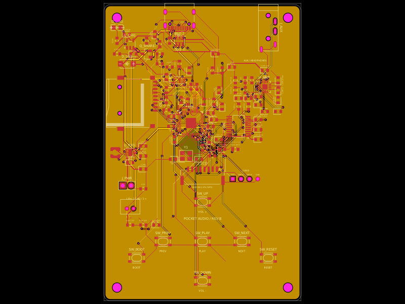 More from this authorDevesh36/pocket-audio-playerA portable, rechargeable microSD audio player built around an RP2040, SPI flash, USB‑C charging/power management, LCD/button controls, PCM5102A I²S DAC, and TPA6132A headphone amplifier in a 3D‑printed enclosure.
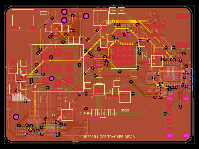 Similar packagepixalynx/nrf9151-gps-trackerA compact 44×32 mm, 4-layer nRF9151 LTE-M/NB-IoT/GNSS tracker PCB with nPM1300 LiPo/USB-C power, nano-SIM/eSIM switching, nRF7002 Wi‑Fi scanning, accelerometer, antennas, buzzer, LEDs, SOS button, and SWD/debug connectors.
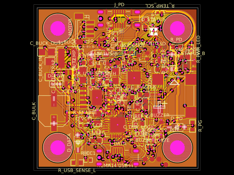 Discover something newAnasSarkiz/NEMA14_CH32X035G8U6A NEMA stepper motor is shown with proposed M3 screws/spacers, four wired motor leads and splices, and a JST SHR-04V-S connector.