Anshgrover23/rfm69-breakout
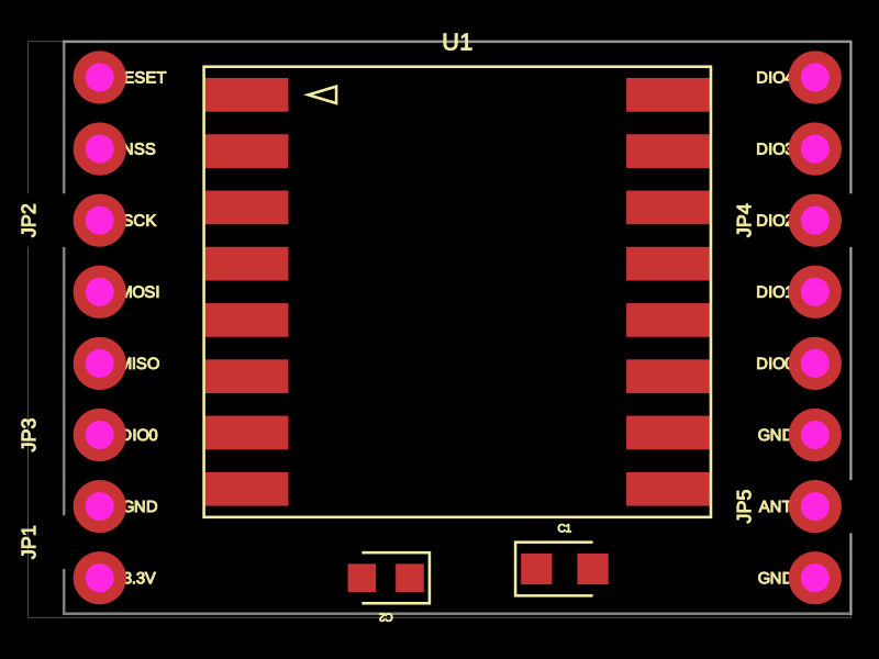
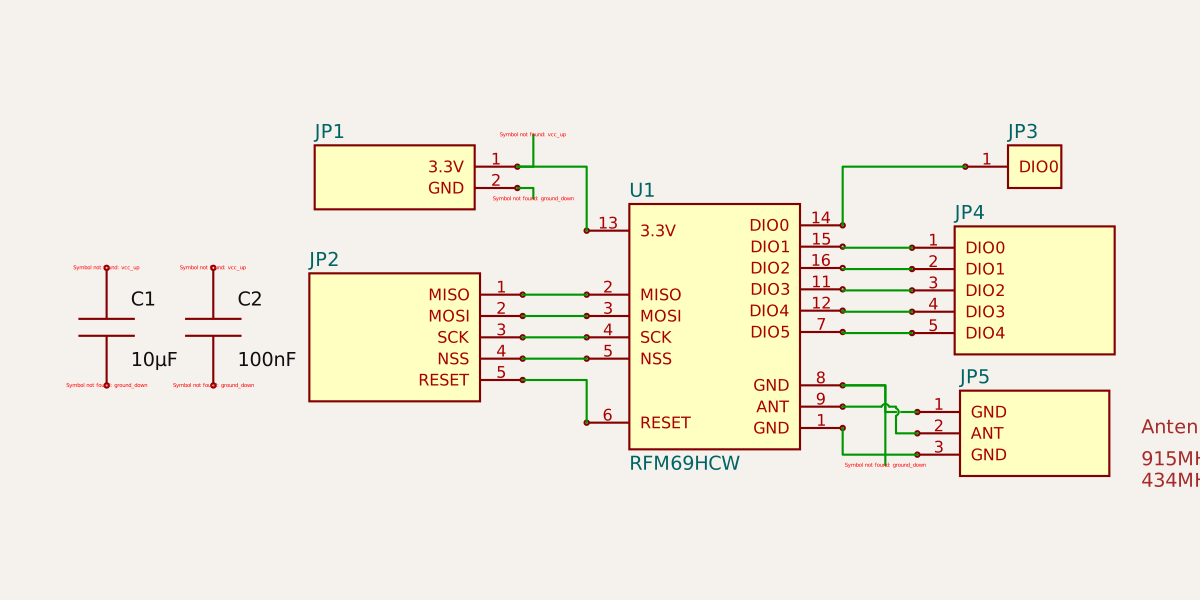
The RFM69HCW module is a 16-pin radio transceiver with SPI and GPIO interfaces, featuring antennas, reset, and data I/O pins.
Usage: To import and use the RFM69HCW component: 1. Import the component: ```tsx import { RFM69HCW } from "@tsci/Anshgrover23.rfm69-breakout" ``` 2. Use in a circuit: ```tsx <board> <RFM69HCW name="RF1" /> </board> ``` The component includes 16 pins with predefined labels like GND, MISO, MOSI, SCK, NSS, RESET, and various DIO pins. You can place it on a board and connect traces to its specific pins using the `sel` selector.
- Version
- 1.0.0
- License
- unset
- Stars
- 1
index.tsx
PCB
Schematic
import { RFM69HCW } from "./RFM69HCW"
import { sel } from "@tscircuit/core"

export default () => (
  <board width="27.94" height="20.32">
    <RFM69HCW
      name="U1"
      footprint="stampboard_left8_right8_bottom0_top0_w18mm_p2.0mm_pw1.2mm_pl3.0mm_padshape=rect"
      pcbY="1.27mm"
    />
    <pinheader
      name="JP1"
      pinCount={2}
      schRotation={180}
      footprint="pinrow2_p2.54_id1.016_od1.88_pinlabeltextalignleft_pinlabelorthogonal_nosquareplating"
      schFacingDirection="right"
      schX={-3}
      schY={1.4}
      pcbRotation={90}
      pcbX={-12.7}
      pcbY={-7.62}
      showSilkscreenPinLabels={true}
      pinLabels={["3.3V", "GND"]}
      connections={{
        pin1: "U1.pin13",
      }}
    />
    <netlabel
      schX={-1.7}
      schY={1.2}
      anchorSide="top"
      net="GND"
      connection="JP1.GND"
    />
    <netlabel
      schX={-1.7}
      schY={1.8}
      net="V3_3"
      connection="JP1.pin1"
      anchorSide="bottom"
    />
    <pinheader
      name="JP2"
      pinCount={5}
      schRotation={0}
      footprint="pinrow5_p2.54_id1.016_od1.88_pinlabeltextalignleft_pinlabelorthogonal_nosquareplating"
      schFacingDirection="right"
      schX={-3}
      schY={-0.1}
      pcbRotation={90}
      pcbX={-12.7}
      pcbY={3.81}
      connections={{
        pin1: sel.U1.pin2,
        pin2: sel.U1.pin3,
        pin3: sel.U1.pin4,
        pin4: sel.U1.pin5,
        pin5: sel.U1.pin6,
      }}
      showSilkscreenPinLabels={true}
      pinLabels={["MISO", "MOSI", "SCK", "NSS", "RESET"]}
    />
    <pinheader
      name="JP3"
      pinCount={1}
      schRotation={180}
      footprint="pinrow1_p2.54_id1.016_od1.88_pinlabeltextalignleft_pinlabelorthogonal_nosquareplating"
      facingDirection="left"
      schX={3}
      schY={1.5}
      pcbRotation={90}
      pcbX={-12.7}
      pcbY={-3.81}
      connections={{
        pin1: sel.U1.pin14,
      }}
      showSilkscreenPinLabels={true}
      pinLabels={["DIO0"]}
      schWidth={0.5}
    />
    <pinheader
      name="JP4"
      pinCount={5}
      schRotation={0}
      footprint="pinrow5_p2.54_id1.016_od1.88_pinlabeltextalignright_pinlabelorthogonal_nosquareplating"
      facingDirection="left"
      schX={3}
      schY={0.34}
      pcbRotation={90}
      pcbX={12.7}
      pcbY={3.81}
      connections={{
        pin1: sel.U1.pin15,
        pin2: sel.U1.pin16,
        pin3: sel.U1.pin11,
        pin4: sel.U1.pin12,
        pin5: sel.U1.pin7,
      }}
      showSilkscreenPinLabels={true}
      pinLabels={["DIO0", "DIO1", "DIO2", "DIO3", "DIO4"]}
    />
    <pinheader
      name="JP5"
      pinCount={3}
      schRotation={180}
      footprint="pinrow3_p2.54_id1.016_od1.88_pinlabeltextalignright_pinlabelorthogonal_nosquareplating"
      facingDirection="left"
      schX={3}
      schY={-1}
      pcbRotation={90}
      pcbX={12.7}
      pcbY={-6.35}
      connections={{
        pin1: sel.U1.pin8,
        pin2: sel.U1.pin9,
        pin3: sel.U1.pin1,
      }}
      showSilkscreenPinLabels={true}
      pinLabels={["GND", "ANT", "GND"]}
    />
    <netlabel
      schX={+1.6}
      schY={-1.3}
      anchorSide="top"
      net="GND"
      connectsTo={["U1.pin8"]}
    />
    <capacitor
      name="C2"
      capacitance={"0.1uF"}
      footprint={"0603"}
      schRotation={90}
      schX={-4.7}
      pcbY={-8.89}
      pcbX={-2.54}
      pcbRotation={180}
      connections={{
        pin1: "net.GND",
        pin2: "net.V3_3",
      }}
    />
    <capacitor
      name="C1"
      capacitance={"10uF"}
      footprint={"1210"}
      schRotation={90}
      schX={-5.7}
      pcbY={-8.57}
      pcbX={3.81}
      connections={{
        pin1: "net.GND",
        pin2: "net.V3_3",
      }}
    />
    <net name="GND" />
    <net name="V3_3" />
    <schematictext
      text="Antenna length (1/4 wave)"
      schX={4}
      schY={-1}
      fontSize={0.2}
      anchor="center_left"
      color="brown"
    />
    <schematictext
      text='915MHz: 3.07" = 78mm'
      schX={4}
      schY={-1.3}
      fontSize={0.2}
      anchor="center_left"
      color="brown"
    />
    <schematictext
      text='434MHz: 6.47" = 164mm'
      schX={4}
      schY={-1.5}
      fontSize={0.2}
      anchor="center_left"
      color="brown"
    />
  </board>
)