AnasSarkiz/vibe_Goblin
These code snippets define various physical electronic components such as ICs, connectors, sensors, LEDs, and chips, specifying their pin layouts, footprint pads, silkscreen markings, courtyard outlines, and 3D CAD models for placement on PCB boards.
- Version
- 1.0.0
- License
- unset
- Stars
- 0
index.circuit.tsx
PCB
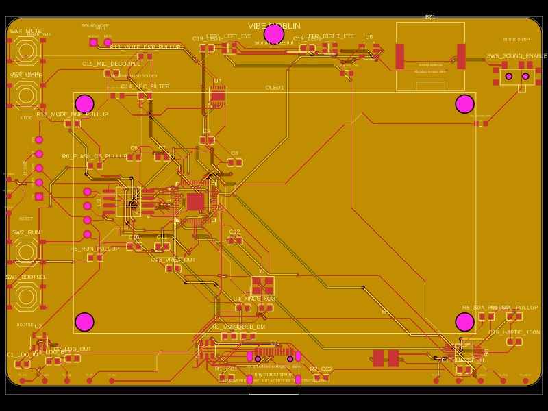
Schematic
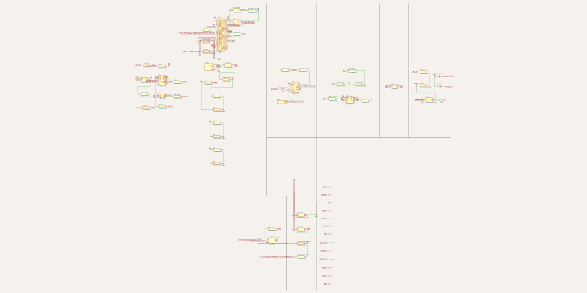
import { A_0603WAF1002T5E as R10K } from "./imports/A_0603WAF1002T5E";
import { A_0603WAF270JT5E as R27 } from "./imports/A_0603WAF270JT5E";
import { A_0603WAF4701T5E as R4K7 } from "./imports/A_0603WAF4701T5E";
import { A_0603WAF5101T5E as R5K1 } from "./imports/A_0603WAF5101T5E";
import { CC0603JRNPO9BN330 as C33P } from "./imports/CC0603JRNPO9BN330";
import { CC0603KRX7R9BB104 as C100N } from "./imports/CC0603KRX7R9BB104";
import { CL10A105KB8NNNC as C1U } from "./imports/CL10A105KB8NNNC";
import { CL10A106KP8NNNC as C10U } from "./imports/CL10A106KP8NNNC";
import { DRV2605LDGSR } from "./imports/DRV2605LDGSR";
import { HS242L03B2C01 } from "./imports/HS242L03B2C01";
import { LCM04084521_B1 } from "./imports/LCM04084521_B1";
import { MAX9814ETD_T } from "./imports/MAX9814ETD_T";
import { ME6211C33M5G_N } from "./imports/ME6211C33M5G_N";
import { PKLCS1212E4001_R1 } from "./imports/PKLCS1212E4001_R1";
import { RP2040 } from "./imports/RP2040";
import { SK_3296S_01_L1 } from "./imports/SK_3296S_01_L1";
import { SN74AHCT1G125DBVR } from "./imports/SN74AHCT1G125DBVR";
import { TS_1187A_B_A_B } from "./imports/TS_1187A_B_A_B";
import { TYPE_C_31_M_12 } from "./imports/TYPE_C_31_M_12";
import { USBLC6_2SC6 } from "./imports/USBLC6_2SC6";
import { W25Q16JVSSIQ } from "./imports/W25Q16JVSSIQ";
import { WS2812B_2020 } from "./imports/WS2812B_2020";
import { X322512MSB4SI } from "./imports/X322512MSB4SI";

const tp = [
	["TP_3V3", "V3_3", -45, -32],
	["TP_VBUS", "VBUS_5V", -41, -32],
	["TP_GND", "GND", -37, -32],
	["TP_DP", "USB_DP", -33, -32],
	["TP_DM", "USB_DM", -29, -32],
	["TP_SDA", "SDA", 29, -32],
	["TP_SCL", "SCL", 33, -32],
	["TP_AUDIO", "AUDIO_ADC", 37, -32],
	["TP_RGB", "RGB_DATA", 41, -32],
	["TP_HAPTIC", "HAPTIC_TRIG", 45, -32],
	["TP_SWDIO", "SWDIO", -47.4, 4],
	["TP_SWCLK", "SWCLK", -47.4, 1],
	["TP_RUN", "RUN", -47.4, -2],
] as const;

function MechanicsAndTestPads() {
	return (
		<>
			<hole name="STRAP1" diameter="3.4mm" pcbX={0} pcbY={30} />
			<silkscreentext
				text="VIBE GOBLIN"
				pcbX={0}
				pcbY={31.5}
				fontSize="1.5mm"
				anchorAlignment="center"
			/>
			<silkscreentext
				text="sound in, buzz out"
				pcbX={0}
				pcbY={28.5}
				fontSize="0.85mm"
				anchorAlignment="center"
			/>
			<silkscreentext
				text="boop to mute"
				pcbX={-42}
				pcbY={30}
				fontSize="0.75mm"
				anchorAlignment="center"
			/>
			<silkscreentext
				text="tiny chaos listener"
				pcbX={0}
				pcbY={-30.8}
				fontSize="0.85mm"
				anchorAlignment="center"
			/>
			<silkscreentext
				text="not a certified emergency alarm"
				pcbX={0}
				pcbY={-29.4}
				fontSize="0.7mm"
				anchorAlignment="center"
			/>
			<silkscreentext
				text="ASSISTIVE PROTOTYPE - NOT A CERTIFIED EMERGENCY ALARM"
				pcbX={0}
				pcbY={-32}
				fontSize="0.6mm"
				anchorAlignment="center"
			/>
			{tp.map(([name, netName, pcbX, pcbY]) => (
				<testpoint
					key={name}
					name={name}
					footprintVariant="pad"
					padShape="circle"
					padDiameter="1mm"
					pcbX={pcbX}
					pcbY={pcbY}
					connections={{ pin1: `net.${netName}` }}
				/>
			))}
		</>
	);
}

function PowerBlock() {
	return (
		<>
			<schematicsection name="USB-C and Power" />
			<TYPE_C_31_M_12
				name="J1"
				pcbX={0}
				pcbY={-29}
				pcbRotation={0}
				schSectionName="USB-C and Power"
			/>
			<USBLC6_2SC6
				name="D1"
				pcbX={-12}
				pcbY={-26.4}
				schSectionName="USB-C and Power"
			/>
			<ME6211C33M5G_N
				name="U2"
				pcbX={-42}
				pcbY={-25}
				schSectionName="USB-C and Power"
			/>
			<R5K1
				name="R1_CC1"
				pcbX={-8.5}
				pcbY={-31.5}
				schSectionName="USB-C and Power"
			/>
			<R5K1
				name="R2_CC2"
				pcbX={8.5}
				pcbY={-31.5}
				schSectionName="USB-C and Power"
			/>
			<R27
				name="R3_USB_DP"
				pcbX={-8}
				pcbY={-24}
				schSectionName="USB-C and Power"
			/>
			<R27
				name="R4_USB_DM"
				pcbX={-4.6}
				pcbY={-24}
				schSectionName="USB-C and Power"
			/>
			<C10U
				name="C1_LDO_IN"
				pcbX={-45}
				pcbY={-29}
				schSectionName="USB-C and Power"
			/>
			<C10U
				name="C2_LDO_OUT"
				pcbX={-36}
				pcbY={-28}
				schSectionName="USB-C and Power"
			/>
			<C100N
				name="C3_LDO_BYP"
				pcbX={-39.5}
				pcbY={-28.5}
				schSectionName="USB-C and Power"
			/>
			<trace from=".J1 > .A1B12" to="net.GND" />
			<trace from=".J1 > .B1A12" to="net.GND" />
			<trace from=".J1 > .EH1" to="net.GND" />
			<trace from=".J1 > .EH2" to="net.GND" />
			<trace from=".J1 > .EH3" to="net.GND" />
			<trace from=".J1 > .EH4" to="net.GND" />
			<trace from=".J1 > .B8" to=".R1_CC1 > .pin1" />
			<trace from=".J1 > .A5" to=".R2_CC2 > .pin1" />
			<trace from=".R1_CC1 > .pin2" to="net.GND" />
			<trace from=".R2_CC2 > .pin2" to="net.GND" />
			<trace from=".J1 > .A8" to="net.VBUS_5V" />
			<trace from=".J1 > .B5" to="net.VBUS_5V" />
			<trace from=".J1 > .A6" to=".D1 > .IO11" />
			<trace from=".J1 > .B6" to=".D1 > .IO12" />
			<trace from=".D1 > .IO21" to=".R3_USB_DP > .pin1" />
			<trace from=".D1 > .IO22" to=".R4_USB_DM > .pin1" />
			<trace from=".R3_USB_DP > .pin2" to="net.USB_DP" />
			<trace from=".R4_USB_DM > .pin2" to="net.USB_DM" />
			<trace from=".D1 > .GND" to="net.GND" />
			<trace from=".D1 > .VBUS" to="net.VBUS_5V" />
			<trace from=".U2 > .VIN" to="net.VBUS_5V" />
			<trace from=".U2 > .CE" to="net.VBUS_5V" />
			<trace from=".U2 > .VSS" to="net.GND" />
			<trace from=".U2 > .VOUT" to="net.V3_3" />
			<trace from=".C1_LDO_IN > .pin1" to="net.VBUS_5V" />
			<trace from=".C1_LDO_IN > .pin2" to="net.GND" />
			<trace from=".C2_LDO_OUT > .pin1" to="net.V3_3" />
			<trace from=".C2_LDO_OUT > .pin2" to="net.GND" />
			<trace from=".C3_LDO_BYP > .pin1" to="net.V3_3" />
			<trace from=".C3_LDO_BYP > .pin2" to="net.GND" />
		</>
	);
}

function RP2040CoreBlock() {
	const decouplers = ["C6", "C7", "C8", "C9", "C10", "C11", "C12"] as const;
	return (
		<>
			<schematicsection name="RP2040 Core" />
			<RP2040
				name="U1"
				pcbX={-14}
				pcbRotation={90}
				pcbY={0}
				schSectionName="RP2040 Core"
			/>
			<W25Q16JVSSIQ
				name="U3"
				pcbX={-26}
				pcbY={0}
				pcbRotation={90}
				schSectionName="RP2040 Core"
			/>
			<X322512MSB4SI
				name="Y1"
				pcbX={-2}
				pcbY={-15}
				schSectionName="RP2040 Core"
			/>
			<TS_1187A_B_A_B
				name="SW1_BOOTSEL"
				pcbX={-44.3}
				pcbY={-17}
				schSectionName="RP2040 Core"
			/>
			<TS_1187A_B_A_B
				name="SW2_RUN"
				pcbX={-44.3}
				pcbY={-9}
				schSectionName="RP2040 Core"
			/>
			<R10K
				name="R5_RUN_PULLUP"
				pcbX={-32}
				pcbY={-10}
				schSectionName="RP2040 Core"
			/>
			<R10K
				name="R6_FLASH_CS_PULLUP"
				pcbX={-32}
				pcbY={6.5}
				schSectionName="RP2040 Core"
			/>
			<C33P name="C4_XIN" pcbX={-5.5} pcbY={-19} schSectionName="RP2040 Core" />
			<C33P
				name="C5_XOUT"
				pcbX={-1.5}
				pcbY={-19}
				schSectionName="RP2040 Core"
			/>
			{decouplers.map((name, i) => (
				<C100N
					key={name}
					name={name}
					pcbX={[-25, -20, -7, -12, -25, -20, -7][i]}
					pcbY={[8, 8, 7, 11, -8, -8, -7][i]}
					schSectionName="RP2040 Core"
				/>
			))}
			<C1U
				name="C13_VREG_OUT"
				pcbX={-18}
				pcbY={-12}
				schSectionName="RP2040 Core"
			/>
			<pinheader
				name="J2_SWD"
				pinCount={5}
				pinLabels={["3V3", "SWDIO", "SWCLK", "RUN", "GND"]}
				showSilkscreenPinLabels
				pcbX={-42}
				pcbRotation={90}
				pcbY={6}
				schSectionName="RP2040 Core"
			/>
			<trace from=".U1 > .GND" to="net.GND" />
			<trace from=".U1 > .TESTEN" to="net.GND" />
			<trace from=".U1 > .IOVDD1" to="net.V3_3" />
			<trace from=".U1 > .IOVDD2" to="net.V3_3" />
			<trace from=".U1 > .IOVDD3" to="net.V3_3" />
			<trace from=".U1 > .IOVDD4" to="net.V3_3" />
			<trace from=".U1 > .IOVDD5" to="net.V3_3" />
			<trace from=".U1 > .IOVDD6" to="net.V3_3" />
			<trace from=".U1 > .USB_VDD" to="net.V3_3" />
			<trace from=".U1 > .ADC_AVDD" to="net.V3_3" />
			<trace from=".U1 > .VREG_IN" to="net.V3_3" />
			<trace from=".U1 > .USB_DP" to="net.USB_DP" />
			<trace from=".U1 > .USB_DM" to="net.USB_DM" />
			<trace from=".U1 > .SWD" to="net.SWDIO" />
			<trace from=".U1 > .SWCLK" to="net.SWCLK" />
			<trace from=".U1 > .RUN" to="net.RUN" />
			<trace from=".R5_RUN_PULLUP > .pin1" to="net.RUN" />
			<trace from=".R5_RUN_PULLUP > .pin2" to="net.V3_3" />
			<trace from=".SW2_RUN > .A" to="net.RUN" />
			<trace from=".SW2_RUN > .B" to="net.GND" />
			<trace from=".SW2_RUN > .C" to="net.RUN" />
			<trace from=".SW2_RUN > .D" to="net.GND" />
			<trace from=".U1 > .QSPI_SS" to=".U3 > .pin1" />
			<trace from=".U1 > .QSPI_SD1" to=".U3 > .pin2" />
			<trace from=".U1 > .QSPI_SD2" to=".U3 > .IO2" />
			<trace from=".U1 > .QSPI_SD0" to=".U3 > .pin5" />
			<trace from=".U1 > .QSPI_SCLK" to=".U3 > .CLK" />
			<trace from=".U1 > .QSPI_SD3" to=".U3 > .IO3" />
			<trace from=".U3 > .VCC" to="net.V3_3" />
			<trace from=".U3 > .GND" to="net.GND" />
			<trace from=".R6_FLASH_CS_PULLUP > .pin1" to=".U3 > .pin1" />
			<trace from=".R6_FLASH_CS_PULLUP > .pin2" to="net.V3_3" />
			<trace from=".SW1_BOOTSEL > .A" to=".U3 > .pin1" />
			<trace from=".SW1_BOOTSEL > .B" to="net.GND" />
			<trace from=".SW1_BOOTSEL > .C" to=".U3 > .pin1" />
			<trace from=".SW1_BOOTSEL > .D" to="net.GND" />
			<trace from=".Y1 > .OSC1" to=".U1 > .XIN" />
			<trace from=".Y1 > .OSC2" to=".U1 > .XOUT" />
			<trace from=".Y1 > .GND1" to="net.GND" />
			<trace from=".Y1 > .GND2" to="net.GND" />
			<trace from=".C4_XIN > .pin1" to=".U1 > .XIN" />
			<trace from=".C4_XIN > .pin2" to="net.GND" />
			<trace from=".C5_XOUT > .pin1" to=".U1 > .XOUT" />
			<trace from=".C5_XOUT > .pin2" to="net.GND" />
			<trace from=".C6 > .pin1" to="net.V3_3" />
			<trace from=".C6 > .pin2" to="net.GND" />
			<trace from=".C7 > .pin1" to="net.V3_3" />
			<trace from=".C7 > .pin2" to="net.GND" />
			<trace from=".C8 > .pin1" to="net.V3_3" />
			<trace from=".C8 > .pin2" to="net.GND" />
			<trace from=".C9 > .pin1" to="net.V3_3" />
			<trace from=".C9 > .pin2" to="net.GND" />
			<trace from=".C10 > .pin1" to="net.V3_3" />
			<trace from=".C10 > .pin2" to="net.GND" />
			<trace from=".C11 > .pin1" to="net.V3_3" />
			<trace from=".C11 > .pin2" to="net.GND" />
			<trace from=".C12 > .pin1" to="net.V3_3" />
			<trace from=".C12 > .pin2" to="net.GND" />
			<trace from=".C13_VREG_OUT > .pin1" to=".U1 > .VREG_VOUT" />
			<trace from=".C13_VREG_OUT > .pin2" to="net.GND" />
			<trace from=".J2_SWD > .3V3" to="net.V3_3" />
			<trace from=".J2_SWD > .SWDIO" to="net.SWDIO" />
			<trace from=".J2_SWD > .SWCLK" to="net.SWCLK" />
			<trace from=".J2_SWD > .RUN" to="net.RUN" />
			<trace from=".J2_SWD > .GND" to="net.GND" />
			<silkscreentext
				text="BOOTSEL"
				pcbX={-44.3}
				pcbY={-22}
				fontSize="0.7mm"
				anchorAlignment="center"
			/>
			<silkscreentext
				text="RESET"
				pcbX={-44.3}
				pcbY={-3}
				fontSize="0.7mm"
				anchorAlignment="center"
			/>
		</>
	);
}

function MicInputBlock() {
	return (
		<>
			<schematicsection name="Microphone Input" />
			<MAX9814ETD_T
				name="U4"
				pcbX={-10}
				pcbY={19}
				schSectionName="Microphone Input"
			/>
			<pinheader
				name="MIC1"
				pinCount={2}
				pitch="2.54mm"
				pinLabels={["MICBIAS", "MICIN"]}
				showSilkscreenPinLabels
				pcbX={-31}
				pcbY={28.5}
				schSectionName="Microphone Input"
			/>
			<resistor
				name="R7_ADC_FILTER_1K"
				resistance="1k"
				footprint="0603"
				supplierPartNumbers={{ jlcpcb: ["C21190"] }}
				pcbX={-28}
				pcbY={19}
				schSectionName="Microphone Input"
			/>
			<C100N
				name="C14_ADC_FILTER"
				pcbX={-23}
				pcbY={19}
				schSectionName="Microphone Input"
			/>
			<C100N
				name="C15_MIC_DECOUPLE"
				pcbX={-29}
				pcbY={23}
				schSectionName="Microphone Input"
			/>
			<trace from=".U4 > .VDD" to="net.V3_3" />
			<trace from=".U4 > .GND" to="net.GND" />
			<trace from=".U4 > .EP" to="net.GND" />
			<trace from=".U4 > .SHDN" to="net.V3_3" />
			<trace from=".U4 > .MICBIAS" to=".MIC1 > .MICBIAS" />
			<trace from=".U4 > .MICIN" to=".MIC1 > .MICIN" />
			<trace from=".U4 > .MICOUT" to=".R7_ADC_FILTER_1K > .pin1" />
			<trace from=".R7_ADC_FILTER_1K > .pin2" to="net.AUDIO_ADC" />
			<trace from=".U1 > .GPIO26_ADC0" to="net.AUDIO_ADC" />
			<trace from=".C14_ADC_FILTER > .pin1" to="net.AUDIO_ADC" />
			<trace from=".C14_ADC_FILTER > .pin2" to="net.GND" />
			<trace from=".C15_MIC_DECOUPLE > .pin1" to="net.V3_3" />
			<trace from=".C15_MIC_DECOUPLE > .pin2" to="net.GND" />
			<silkscreentext
				text="SOUND HOLE"
				pcbX={-32}
				pcbY={31.5}
				fontSize="0.75mm"
				anchorAlignment="center"
			/>
			<silkscreentext
				text="MIC1 DNP / HAND SOLDER"
				pcbX={-25}
				pcbY={22.5}
				fontSize="0.65mm"
				anchorAlignment="center"
			/>
		</>
	);
}

function HapticBlock() {
	return (
		<>
			<schematicsection name="Haptic Vibration" />
			<DRV2605LDGSR
				name="U5"
				pcbX={34}
				pcbY={-27}
				pcbRotation={270}
				schSectionName="Haptic Vibration"
			/>
			<LCM04084521_B1
				name="M1"
				pcbX={20}
				pcbY={-28}
				schSectionName="Haptic Vibration"
			/>
			<R4K7
				name="R8_SDA_PULLUP"
				pcbX={38}
				pcbY={-20.5}
				schSectionName="Haptic Vibration"
			/>
			<R4K7
				name="R9_SCL_PULLUP"
				pcbX={43}
				pcbY={-20.5}
				schSectionName="Haptic Vibration"
			/>
			<C100N
				name="C16_HAPTIC_100N"
				pcbX={43}
				pcbY={-25}
				schSectionName="Haptic Vibration"
			/>
			<C1U
				name="C17_HAPTIC_1U"
				pcbX={34}
				pcbY={-30}
				schSectionName="Haptic Vibration"
			/>
			<trace from=".U5 > .SDA" to="net.SDA" />
			<trace from=".U5 > .SCL" to="net.SCL" />
			<trace from=".U5 > .VDD" to="net.V3_3" />
			<trace from=".U5 > .REG" to="net.V3_3" />
			<trace from=".U5 > .EN" to="net.V3_3" />
			<trace from=".U5 > .GND" to="net.GND" />
			<trace from=".U5 > .OUT_POS" to=".M1 > .pin1" />
			<trace from=".U5 > .OUT_NEG" to=".M1 > .pin2" />
			<trace from=".R8_SDA_PULLUP > .pin1" to="net.SDA" />
			<trace from=".R8_SDA_PULLUP > .pin2" to="net.V3_3" />
			<trace from=".R9_SCL_PULLUP > .pin1" to="net.SCL" />
			<trace from=".R9_SCL_PULLUP > .pin2" to="net.V3_3" />
			<trace from=".C16_HAPTIC_100N > .pin1" to="net.V3_3" />
			<trace from=".C16_HAPTIC_100N > .pin2" to="net.GND" />
			<trace from=".C17_HAPTIC_1U > .pin1" to="net.V3_3" />
			<trace from=".C17_HAPTIC_1U > .pin2" to="net.GND" />
			<trace from=".U1 > .GPIO4" to="net.SDA" />
			<trace from=".U1 > .GPIO5" to="net.SCL" />
		</>
	);
}

function OledFaceBlock() {
	return (
		<>
			<schematicsection name="OLED Face" />
			<HS242L03B2C01
				name="OLED1"
				pcbX={0}
				pcbY={-2}
				schSectionName="OLED Face"
			/>
			<trace from=".OLED1 > .GND" to="net.GND" />
			<trace from=".OLED1 > .VCC" to="net.V3_3" />
			<trace from=".OLED1 > .SDA" to="net.SDA" />
			<trace from=".OLED1 > .SCL" to="net.SCL" />
		</>
	);
}

function RgbEyesBlock() {
	return (
		<>
			<schematicsection name="RGB Eyes" />
			<SN74AHCT1G125DBVR
				name="U6"
				pcbX={17}
				pcbY={27}
				schSectionName="RGB Eyes"
			/>
			<WS2812B_2020
				name="LED1_LEFT_EYE"
				pcbX={-8}
				pcbY={27.5}
				schSectionName="RGB Eyes"
			/>
			<WS2812B_2020
				name="LED2_RIGHT_EYE"
				pcbX={10}
				pcbY={27.5}
				schSectionName="RGB Eyes"
			/>
			<resistor
				name="R10_RGB_DATA_330R"
				resistance="330"
				footprint="0603"
				supplierPartNumbers={{ jlcpcb: ["C23138"] }}
				pcbX={13}
				pcbY={23}
				schSectionName="RGB Eyes"
			/>
			<C100N name="C18_LED1" pcbX={-12} pcbY={27.5} schSectionName="RGB Eyes" />
			<C100N name="C19_LED2" pcbX={6} pcbY={27.5} schSectionName="RGB Eyes" />
			<trace from=".U1 > .GPIO6" to=".U6 > .A" />
			<trace from=".U6 > .VCC" to="net.VBUS_5V" />
			<trace from=".U6 > .GND" to="net.GND" />
			<trace from=".U6 > .OE" to="net.GND" />
			<trace from=".U6 > .Y" to=".R10_RGB_DATA_330R > .pin1" />
			<trace from=".R10_RGB_DATA_330R > .pin2" to="net.RGB_DATA" />
			<trace from=".LED1_LEFT_EYE > .pin1" to="net.VBUS_5V" />
			<trace from=".LED1_LEFT_EYE > .pin2" to="net.RGB_DATA" />
			<trace from=".LED1_LEFT_EYE > .pin3" to="net.GND" />
			<trace from=".LED1_LEFT_EYE > .pin4" to=".LED2_RIGHT_EYE > .pin2" />
			<trace from=".LED2_RIGHT_EYE > .pin1" to="net.VBUS_5V" />
			<trace from=".LED2_RIGHT_EYE > .pin3" to="net.GND" />
			<trace from=".LED2_RIGHT_EYE > .pin4" to="net.NO_CONNECT_LED2_DOUT" />
			<trace from=".C18_LED1 > .pin1" to="net.VBUS_5V" />
			<trace from=".C18_LED1 > .pin2" to="net.GND" />
			<trace from=".C19_LED2 > .pin1" to="net.VBUS_5V" />
			<trace from=".C19_LED2 > .pin2" to="net.GND" />
		</>
	);
}

function OptionalBuzzerBlock() {
	return (
		<>
			<schematicsection name="Optional Buzzer" />
			<PKLCS1212E4001_R1
				name="BZ1"
				pcbX={28}
				pcbY={26}
				schSectionName="Optional Buzzer"
			/>
			<SK_3296S_01_L1
				name="SW5_SOUND_ENABLE"
				pcbX={43.5}
				pcbY={23}
				schSectionName="Optional Buzzer"
			/>
			<resistor
				name="R11_BUZZER_470R"
				resistance="470"
				footprint="0603"
				supplierPartNumbers={{ jlcpcb: ["C23179"] }}
				pcbX={37}
				pcbY={14}
				schSectionName="Optional Buzzer"
			/>
			<trace from=".U1 > .GPIO15" to=".R11_BUZZER_470R > .pin1" />
			<trace from=".R11_BUZZER_470R > .pin2" to=".SW5_SOUND_ENABLE > .pin2" />
			<trace from=".SW5_SOUND_ENABLE > .pin1" to=".BZ1 > ._POS" />
			<trace from=".BZ1 > ._NEG" to="net.GND" />
			<trace from=".SW5_SOUND_ENABLE > .pin3" to="net.NO_CONNECT_SOUND_OFF" />
			<silkscreentext
				text="SOUND ON/OFF"
				pcbX={43.5}
				pcbY={29}
				fontSize="0.65mm"
				anchorAlignment="center"
			/>
			<silkscreentext
				text="sound optional"
				pcbX={28}
				pcbY={24.5}
				fontSize="0.65mm"
				anchorAlignment="center"
			/>
			<silkscreentext
				text="vibration is main alert"
				pcbX={28}
				pcbY={23.3}
				fontSize="0.6mm"
				anchorAlignment="center"
			/>
		</>
	);
}

function ButtonBlock() {
	return (
		<>
			<schematicsection name="Buttons" />
			<TS_1187A_B_A_B
				name="SW3_MODE"
				pcbX={-44.3}
				pcbY={19}
				schSectionName="Buttons"
			/>
			<TS_1187A_B_A_B
				name="SW4_MUTE"
				pcbX={-44.3}
				pcbY={27}
				schSectionName="Buttons"
			/>
			<R10K
				name="R12_MODE_DNP_PULLUP"
				pcbX={-36}
				pcbY={14}
				doNotPlace
				schSectionName="Buttons"
			/>
			<R10K
				name="R13_MUTE_DNP_PULLUP"
				pcbX={-23}
				pcbY={26}
				doNotPlace
				schSectionName="Buttons"
			/>
			<trace from=".SW3_MODE > .A" to=".U1 > .GPIO10" />
			<trace from=".SW3_MODE > .B" to="net.GND" />
			<trace from=".SW3_MODE > .C" to=".U1 > .GPIO10" />
			<trace from=".SW3_MODE > .D" to="net.GND" />
			<trace from=".SW4_MUTE > .A" to=".U1 > .GPIO11" />
			<trace from=".SW4_MUTE > .B" to="net.GND" />
			<trace from=".SW4_MUTE > .C" to=".U1 > .GPIO11" />
			<trace from=".SW4_MUTE > .D" to="net.GND" />
			<trace from=".R12_MODE_DNP_PULLUP > .pin1" to=".U1 > .GPIO10" />
			<trace from=".R12_MODE_DNP_PULLUP > .pin2" to="net.V3_3" />
			<trace from=".R13_MUTE_DNP_PULLUP > .pin1" to=".U1 > .GPIO11" />
			<trace from=".R13_MUTE_DNP_PULLUP > .pin2" to="net.V3_3" />
			<silkscreentext
				text="MODE"
				pcbX={-44.3}
				pcbY={15}
				fontSize="0.7mm"
				anchorAlignment="center"
			/>
			<silkscreentext
				text="BOOP / MUTE"
				pcbX={-44.3}
				pcbY={23}
				fontSize="0.7mm"
				anchorAlignment="center"
			/>
		</>
	);
}

export default function VibeGoblinRp2040Mini() {
	return (
		<board
			title="Vibe Goblin RP2040 Mini"
			width="96mm"
			height="66mm"
			layers={4}
			borderRadius="3mm"
		>
			{/*
        Firmware notes: sample GPIO26/ADC0 microphone audio, compute envelope/RMS,
        classify short peaks as KNOCK?, repeated peaks as CHECK, and sustained loud
        sound as LOUD!. KNOCK uses 3 short vibrations, OLED text, yellow flashes,
        and optional soft beeps. LOUD uses one strong vibration, OLED LOUD!, red
        flash, and optional beep. REPEATED pulses vibration with OLED CHECK and
        purple/blue LEDs. MUTE disables sound; vibration, OLED, and LEDs remain.
        Default boot should be sound-off or low-volume mixed mode. This is an
        assistive prototype, not a certified smoke/fire/medical/emergency alarm.
      */}
			<MechanicsAndTestPads />
			<PowerBlock />
			<RP2040CoreBlock />
			<MicInputBlock />
			<HapticBlock />
			<OledFaceBlock />
			<RgbEyesBlock />
			<OptionalBuzzerBlock />
			<ButtonBlock />
			<copperpour name="GND_PLANE_L2" layer="inner1" connectsTo="net.GND" />
			<copperpour name="POWER_PLANE_L3" layer="inner2" connectsTo="net.V3_3" />
		</board>
	);
}