AnasSarkiz/usb-c-pwm-pa25
A component library defining an AO3400A N-channel MOSFET, 47 µF polarized capacitor, 3-pin through-hole connector, and 9.1 V Zener diode with PCB footprints and 3D CAD models.
- Version
- 0.1.0-prototype.2
- License
- unset
- Stars
- 0
tests/board.test.ts
import { expect, test } from "bun:test";
import { file } from "bun";
import {
	any_source_component,
	source_net,
	source_port,
	pcb_via,
	pcb_trace,
	schematic_sheet,
} from "circuit-json";
import { z } from "zod";

const records = z
	.array(z.object({ type: z.string() }).passthrough())
	.parse(
		await file(new URL("../dist/index/circuit.json", import.meta.url)).json(),
	);
const components = records
	.filter((r) => r.type === "source_component")
	.map((r) => any_source_component.parse(r))
	.filter((component) => component.type === "source_component");
const ports = records
	.filter((r) => r.type === "source_port")
	.map((r) => source_port.parse(r));
const nets = records
	.filter((r) => r.type === "source_net")
	.map((r) => source_net.parse(r));
const vias = records
	.filter((r) => r.type === "pcb_via")
	.map((r) => pcb_via.parse(r));
const sheets = records
	.filter((r) => r.type === "schematic_sheet")
	.map((r) => schematic_sheet.parse(r));

function connectedNet(componentName: string, pin: string) {
	const component = components.find((c) => c.name === componentName);
	if (!component) throw new Error(`Missing component ${componentName}`);
	const port = ports.find(
		(p) =>
			p.source_component_id === component.source_component_id &&
			p.port_hints?.includes(pin),
	);
	if (!port?.subcircuit_connectivity_map_key)
		throw new Error(`Unconnected ${componentName}.${pin}`);
	const net = nets.find(
		(n) =>
			n.subcircuit_connectivity_map_key ===
			port.subcircuit_connectivity_map_key,
	);
	if (!net) throw new Error(`Unnamed connection on ${componentName}.${pin}`);
	return net.name;
}

test("power must pass PD negotiation, input protection, regulation, and reverse blocking", () => {
	expect(connectedNet("U1", "PPHV1")).toBe("PD_OUT");
	expect(connectedNet("U2", "IN")).toBe("PD_OUT");
	expect(connectedNet("U2", "OUT")).toBe("V15");
	expect(connectedNet("U4", "VIN")).toBe("V15");
	expect(connectedNet("L1", "pin2")).toBe("V12_BUCK");
	expect(connectedNet("U5", "IN")).toBe("V12_BUCK");
	expect(connectedNet("U5", "OUT")).toBe("VM");
	expect(connectedNet("U6", "VM")).toBe("VM");
	expect(connectedNet("C23", "pin1")).toBe("VM");
});

test("hardware faults override the firmware drive request and reset defaults disable power", () => {
	for (const [name, pin] of [
		["U2", "FLT"],
		["U2", "AUXOFF"],
		["U5", "FLT"],
		["U5", "AUXOFF"],
		["U6", "nFAULT"],
		["U8", "OUT_B"],
		["U10", "B"],
	]) {
		expect(connectedNet(name, pin)).toBe("HEALTH");
	}
	expect(connectedNet("U10", "Y")).toBe(connectedNet("U6", "nSLEEP"));
	expect(connectedNet("Q2", "D")).toBe(connectedNet("U2", "EN_UVLO"));
	expect(connectedNet("Q3", "D")).toBe(connectedNet("U5", "EN_UVLO"));
	expect(connectedNet("R15", "pin1")).toBe("V3V3");
	expect(connectedNet("R15", "pin2")).toBe(connectedNet("Q2", "G"));
	for (const name of ["R33", "R34", "R55", "R61"])
		expect(connectedNet(name, "pin2")).toBe("GND");
});

test("both USB orientations, gate protection, motor polarity and standard JST SWD", () => {
	for (const cc of ["CC1", "CC2"])
		expect(connectedNet("J1", cc)).toBe(connectedNet("U1", cc));
	expect(connectedNet("D2", "IO1")).toBe("CC1");
	expect(connectedNet("D2", "IO2")).toBe("CC2");
	expect(connectedNet("D6", "cathode")).toBe("CLAMP_GATE");
	expect(connectedNet("D6", "anode")).toBe("GND");
	expect(connectedNet("J2", "pin1")).toBe(connectedNet("U6", "OUT1"));
	expect(connectedNet("J2", "pin2")).toBe(connectedNet("U6", "OUT2"));
	for (const [index, net] of [
		"V3V3",
		"SWDIO",
		"GND",
		"SWCLK",
		"NRST",
	].entries())
		expect(connectedNet("J5", `pin${index + 1}`)).toBe(net);
});

test("MOSFET and shunt-reference symbols retain the manufacturer's physical pin numbers", () => {
	for (const [name, gate, drain] of [
		["Q1", "CLAMP_GATE", "BRAKE_DRAIN"],
		["Q2", "PWR_OFF", "INPUT_EN"],
		["Q3", "PWR_OFF", "MOTOR_UV"],
	]) {
		expect(connectedNet(name, "pin1")).toBe(gate);
		expect(connectedNet(name, "pin2")).toBe("GND");
		expect(connectedNet(name, "pin3")).toBe(drain);
	}
	expect(connectedNet("U7", "pin1")).toBe("VREF_2V5");
	expect(connectedNet("U7", "pin2")).toBe("GND");
	expect(connectedNet("U7", "pin3")).toBe("GND");
});

test("six native A4 sheets and exact supplier identities for every assembled part", () => {
	expect(sheets).toHaveLength(6);
	for (const sheet of sheets) {
		expect(sheet.sheet_size).toBe("a4");
		expect(sheet.sheet_width).toBe(297);
		expect(sheet.sheet_height).toBe(210);
	}
	for (const component of components.filter(
		(c) => !/^(TP|H|FID)/.test(c.name),
	)) {
		expect(component.manufacturer_part_number, component.name).toBeTruthy();
		expect(
			component.supplier_part_numbers?.jlcpcb?.[0],
			component.name,
		).toMatch(/^C\d+$/);
	}
});

// Validate the actual geometric fields, including native fiducials whose
// pcb_component_id is null. circuit-json 0.0.499's full metadata schema does not
// accept that native output or numeric display offsets; geometry is independent.
const point = z.object({ x: z.number(), y: z.number() });
const rect = point.extend({
	width: z.number().positive(),
	height: z.number().positive(),
});
const padGeometry = z.discriminatedUnion("shape", [
	rect.extend({ shape: z.literal("rect") }),
	rect.extend({ shape: z.literal("pill"), radius: z.number().positive() }),
	point.extend({ shape: z.literal("circle"), radius: z.number().positive() }),
	z.object({ shape: z.literal("polygon"), points: z.array(point).min(3) }),
]);
const pads = records
	.filter((r) => r.type === "pcb_smtpad")
	.map((r) => ({ id: r.pcb_smtpad_id, geometry: padGeometry.parse(r) }));
type Point = z.infer<typeof point>;
type Pad = z.infer<typeof padGeometry>;

function segmentDistance(point: Point, ends: readonly [Point, Point]) {
	const [start, end] = ends;
	const dx = end.x - start.x,
		dy = end.y - start.y;
	const lengthSquared = dx * dx + dy * dy;
	const fraction =
		lengthSquared === 0
			? 0
			: Math.max(
					0,
					Math.min(
						1,
						((point.x - start.x) * dx + (point.y - start.y) * dy) /
							lengthSquared,
					),
				);
	return Math.hypot(
		point.x - start.x - fraction * dx,
		point.y - start.y - fraction * dy,
	);
}

function padDistance(position: Point, pad: Pad) {
	if (pad.shape === "circle")
		return Math.max(
			0,
			Math.hypot(position.x - pad.x, position.y - pad.y) - pad.radius,
		);
	if (pad.shape === "rect")
		return Math.hypot(
			Math.max(0, Math.abs(position.x - pad.x) - pad.width / 2),
			Math.max(0, Math.abs(position.y - pad.y) - pad.height / 2),
		);
	if (pad.shape === "pill") {
		const horizontal = pad.width >= pad.height;
		const halfStraight = (Math.max(pad.width, pad.height) - 2 * pad.radius) / 2;
		return Math.max(
			0,
			segmentDistance(position, [
				{
					x: pad.x - (horizontal ? halfStraight : 0),
					y: pad.y - (horizontal ? 0 : halfStraight),
				},
				{
					x: pad.x + (horizontal ? halfStraight : 0),
					y: pad.y + (horizontal ? 0 : halfStraight),
				},
			]) - pad.radius,
		);
	}
	let inside = false,
		distance = Infinity;
	for (
		let index = 0, previous = pad.points.length - 1;
		index < pad.points.length;
		previous = index++
	) {
		const a = pad.points[index],
			b = pad.points[previous];
		if (
			a.y > position.y !== b.y > position.y &&
			position.x < ((b.x - a.x) * (position.y - a.y)) / (b.y - a.y) + a.x
		)
			inside = !inside;
		distance = Math.min(distance, segmentDistance(position, [a, b]));
	}
	return inside ? 0 : distance;
}

test("ordinary via holes clear every SMT pad, including same-net pads", () => {
	expect(vias.length).toBeGreaterThanOrEqual(4);
	for (const via of vias) {
		expect(via.hole_diameter).toBeGreaterThanOrEqual(0.3);
		expect(via.outer_diameter - via.hole_diameter).toBeGreaterThanOrEqual(
			0.29999,
		);
		expect(via.layers).toEqual(["top", "inner1", "inner2", "bottom"]);
		for (const pad of pads)
			expect(
				padDistance(via, pad.geometry) - via.hole_diameter / 2,
				`${via.pcb_via_id} / ${pad.id}`,
			).toBeGreaterThanOrEqual(0.19999);
	}
});

test("no unresolved native error records", () => {
	expect(records.filter((r) => r.type.endsWith("_error"))).toEqual([]);
});

test("generated copper respects the 0.15 mm minimum signal width", () => {
	for (const trace of records
		.filter((record) => record.type === "pcb_trace")
		.map((record) => pcb_trace.parse(record))) {
		for (const point of trace.route) {
			if (point.route_type !== "wire") continue;
			expect(point.width, trace.pcb_trace_id).toBeGreaterThanOrEqual(0.14999);
		}
	}
});
Related Packages
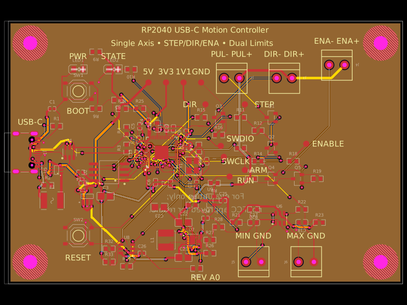 More from this authorAnasSarkiz/rp2040-usb-c-single-axis-dm542t-motion-controller--01a0e89cA USB‑C RP2040 controller board with external QSPI flash, crystal clock, regulated 3.3/1.1/5 V power, boost-converted motor-driver supply, protected USB and limit inputs, status LEDs, reset/boot switches, and AO3400A MOSFET outputs for stepper-control signals.
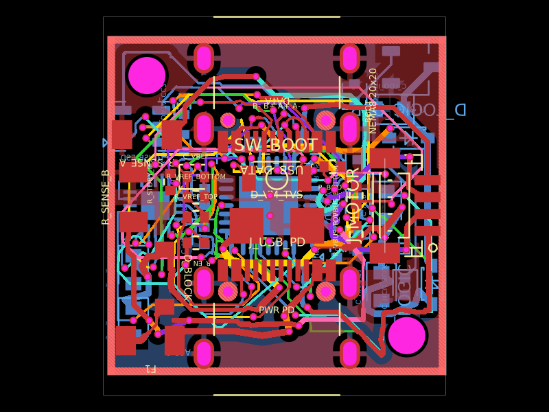 Similar packageShiboSoftwareDev/nema8-20mm-dual-usbc-stepper-controllerBAT54C is a compact three-pin SMD dual Schottky diode, while BAT54WS is a two-pin SMD single Schottky diode, each with defined PCB footprints and 3D models.
 Discover something newpixalynx/usb3-hub-10gA USB 3.2 Gen 2 six-port hub board with USB-C PD power input, regulated 5 V/3.3 V/1.15 V rails, one upstream and four protected downstream USB-A/USB-C ports, SuperSpeed muxes, ESD protection, and controlled port power.