AnasSarkiz/usb-c-pwm-pa25
A component library defining an AO3400A N-channel MOSFET, 47 µF polarized capacitor, 3-pin through-hole connector, and 9.1 V Zener diode with PCB footprints and 3D CAD models.
- Version
- 0.1.0-prototype.2
- License
- unset
- Stars
- 0
lib/rail-clamp.tsx
import { SchematicNote } from "./schematic-note";
import { AO3400A } from "../imports/AO3400A";
import { LM393BIDR } from "../imports/LM393BIDR";
import { LM4040B25IDBZR } from "../imports/LM4040B25IDBZR";
import { BZT52C9V1_7_F } from "../imports/BZT52C9V1_7_F";
import { CRM2512AJW_201ELF } from "../imports/CRM2512AJW_201ELF";
import { C, R, TestPad } from "./passives";

const brakePositions = [
	[5, 20],
	[13.5, 20],
	[22, 20],
	[30.5, 20],
	[5, 26],
	[13.5, 26],
	[22, 26],
	[30.5, 26],
] as const;

export function RailClamp() {
	return (
		<schematicsheet
			name="clamp"
			displayName="04 Regeneration clamp and temperature interlock — A1 prototype"
			sheetSize="A4"
			sheetIndex={3}
		>
			<LM4040B25IDBZR
				name="U7"
				pcbX={21}
				pcbY={10}
				schX={-10}
				schY={4}
				connections={{ C: "net.VREF_2V5", A: "net.GND", pin3: "net.GND" }}
			/>
			<R
				name="R40"
				resistance="4.7k"
				pcb={[17, 11]}
				sch={[-10, 7]}
				nets={["VM", "VREF_2V5"]}
			/>
			<C
				name="C30"
				capacitance="100nF"
				pcb={[21, 13.5]}
				sch={[-10, 0.5]}
				nets={["VREF_2V5", "GND"]}
			/>
			<SchematicNote
				schX={-9.5}
				schY={8.8}
				fontSize={0.23}
				text={
					"U7: 2.5 V shunt reference, 0.2% initial accuracy.\nPowered from VM so the clamp works after USB removal.\n4.7 kΩ bias ≈2 mA at 12 V; also sets motor current limit."
				}
			/>
			<LM393BIDR
				name="U8"
				pcbX={29}
				pcbY={11}
				schX={0}
				schY={4}
				connections={{
					VCC: "net.VM",
					GND: "net.GND",
					IN_A_PLUS: "net.CLAMP_SENSE",
					IN_A_MINUS: "net.VREF_2V5",
					OUT_A: "net.CLAMP_GATE",
					IN_B_PLUS: "net.TEMP_ADC",
					IN_B_MINUS: "net.TEMP_REF",
					OUT_B: "net.HEALTH",
				}}
			/>
			<SchematicNote
				schX={1}
				schY={8.8}
				fontSize={0.23}
				text={
					"U8: VM-powered dual open-collector comparator, 2–36 V.\nA: hysteretic shunt, nominal ON 13.43 V / OFF ≈12.95 V.\nB: NTC overtemperature directly inhibits the driver.\nThresholds and pulse-energy capacity require prototype verification."
				}
			/>
			<C
				name="C31"
				capacitance="100nF"
				pcb={[34, 12]}
				sch={[7, 7]}
				nets={["VM", "GND"]}
			/>
			<R
				name="R41"
				resistance="43.2k"
				pcb={[25, 15.5]}
				sch={[-5, 0]}
				nets={["VM", "CLAMP_SENSE"]}
			/>
			<R
				name="R42"
				resistance="10k"
				pcb={[29, 15.5]}
				sch={[0, 0]}
				nets={["CLAMP_SENSE", "GND"]}
			/>
			<R
				name="R43"
				rotation={180}
				resistance="820k"
				pcb={[33, 15.5]}
				sch={[5, 0]}
				nets={["CLAMP_GATE", "CLAMP_SENSE"]}
			/>
			<C
				name="C32"
				capacitance="330pF"
				pcb={[34.7, 9.6]}
				sch={[10, 0]}
				nets={["CLAMP_SENSE", "GND"]}
			/>
			<R
				name="R44"
				resistance="10k"
				pcb={[38, 13]}
				sch={[7, 4.5]}
				nets={["VM", "CLAMP_GATE"]}
			/>
			<R
				name="R45"
				rotation={180}
				resistance="100k"
				pcb={[38, 10.5]}
				sch={[12, 4.5]}
				nets={["CLAMP_GATE", "GND"]}
			/>
			<BZT52C9V1_7_F
				name="D6"
				pcbX={39}
				pcbY={7}
				schX={12}
				schY={7}
				schRotation={90}
				connections={{ anode: "net.GND", cathode: "net.CLAMP_GATE" }}
			/>
			<AO3400A
				name="Q1"
				pcbX={38}
				pcbY={16.5}
				schX={10}
				schY={-4}
				connections={{
					G: "net.CLAMP_GATE",
					D: "net.BRAKE_DRAIN",
					S: "net.GND",
				}}
			/>
			{brakePositions.map((pcb, index) => (
				<CRM2512AJW_201ELF
					key={index}
					name={`R${70 + index}`}
					pcbX={pcb[0]}
					pcbY={pcb[1]}
					schRotation={-90}
					schX={-11 + (index % 4) * 4.8}
					schY={-3.2 - Math.floor(index / 4) * 2.4}
					connections={{ pin1: "net.VM", pin2: "net.BRAKE_DRAIN" }}
				/>
			))}
			<R
				name="R46"
				resistance="27.4k"
				pcb={[17, 14]}
				sch={[-10, -8]}
				nets={["V3V3", "TEMP_ADC"]}
			/>
			<resistor
				name="R78"
				resistance="10k"
				footprint="0603"
				manufacturerPartNumber="NCP18XH103F03RB"
				supplierPartNumbers={{ jlcpcb: ["C13564"] }}
				pcbX={22}
				pcbY={6.5}
				schX={-5}
				schY={-8}
				schRotation={-90}
				connections={{ pin1: "net.TEMP_ADC", pin2: "net.GND" }}
			/>
			<R
				name="R47"
				resistance="240k"
				pcb={[25, 5.9]}
				sch={[0, -8]}
				nets={["VREF_2V5", "TEMP_REF"]}
			/>
			<R
				name="R48"
				resistance="26.7k"
				pcb={[33, 5.5]}
				sch={[5, -8]}
				nets={["TEMP_REF", "GND"]}
			/>
			<C
				name="C33"
				capacitance="100nF"
				pcb={[16, 16.5]}
				sch={[10, -8]}
				nets={["TEMP_ADC", "GND"]}
			/>
			<SchematicNote
				schX={0}
				schY={-11}
				fontSize={0.23}
				text={
					"R70–R77: 8 × 200 Ω / 2 W in parallel = 25 Ω, ±5%; ≈7.84 W total at 14 V.\nInitial supervised-test envelope: ≤0.5 J/event, ≤1 W average; these are qualification targets.\nR78: 10 kΩ NTC B25/50=3380 K. Hardware trip around 70°C; firmware trips earlier.\nNo continuous externally driven load. Safe reversal coast time must be measured."
				}
			/>
			<TestPad name="TP9" net="VREF_2V5" pcb={[13, 12]} sch={[-14, 2]} />
			<TestPad name="TP10" net="CLAMP_GATE" pcb={[41, 13]} sch={[14, -4]} />
		</schematicsheet>
	);
}
Related Packages
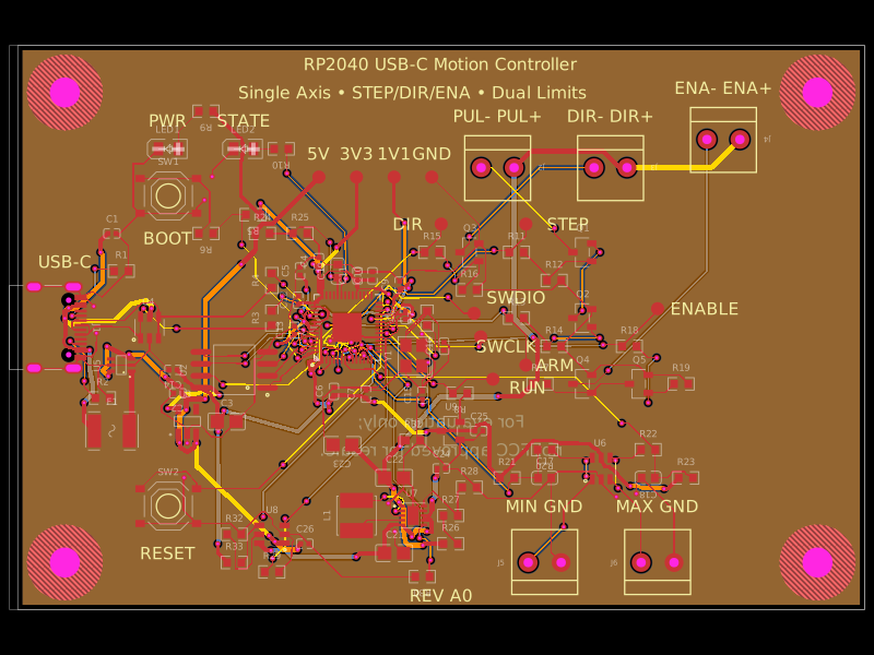 More from this authorAnasSarkiz/rp2040-usb-c-single-axis-dm542t-motion-controller--01a0e89cA USB‑C RP2040 controller board with external QSPI flash, crystal clock, regulated 3.3/1.1/5 V power, boost-converted motor-driver supply, protected USB and limit inputs, status LEDs, reset/boot switches, and AO3400A MOSFET outputs for stepper-control signals.
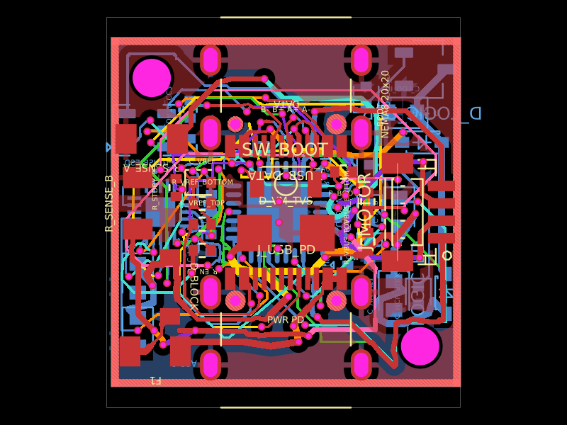 Similar packageShiboSoftwareDev/nema8-20mm-dual-usbc-stepper-controllerBAT54C is a compact three-pin SMD dual Schottky diode, while BAT54WS is a two-pin SMD single Schottky diode, each with defined PCB footprints and 3D models.
 Discover something newpixalynx/usb3-hub-10gA USB 3.2 Gen 2 six-port hub board with USB-C PD power input, regulated 5 V/3.3 V/1.15 V rails, one upstream and four protected downstream USB-A/USB-C ports, SuperSpeed muxes, ESD protection, and controlled port power.