AnasSarkiz/usb-c-pwm-pa25
A component library defining an AO3400A N-channel MOSFET, 47 µF polarized capacitor, 3-pin through-hole connector, and 9.1 V Zener diode with PCB footprints and 3D CAD models.
- Version
- 0.1.0-prototype.2
- License
- unset
- Stars
- 0
lib/controller.tsx
import { SchematicNote } from "./schematic-note";
import { STM32C011F4P6 } from "../imports/STM32C011F4P6";
import { SN74LVC1G08DBVR } from "../imports/SN74LVC1G08DBVR";
import { S5B_PH_SM4_TB_LF__SN_ } from "../imports/S5B_PH_SM4_TB_LF__SN_";
import { C, R, TestPad } from "./passives";

export function Controller() {
	return (
		<schematicsheet
			name="controller"
			displayName="05 Control and standard JST SWD — A1 prototype"
			sheetSize="A4"
			sheetIndex={4}
		>
			<STM32C011F4P6
				name="U9"
				pcbX={0}
				pcbY={-15.5}
				schX={0}
				schY={3}
				connections={{
					VDD: "net.V3V3",
					GND: "net.GND",
					PF2_NRST: "net.NRST",
					PB7: "net.SDA",
					PB6: "net.SCL",
					PC14_OSCX_IN: "net.FWD",
					PC15_OSCX_OUT: "net.REV",
					PA0: "net.POT_ADC",
					PA1: "net.CURRENT_ADC",
					PA2: "net.VM_ADC",
					PA3: "net.TEMP_ADC",
					PA4: "net.PWM",
					PA5: "net.DIR",
					PA6: "net.MCU_ENABLE",
					PA7: "net.LED_FAULT",
					PA8: "net.HEALTH",
					PA11: "net.PWR_OFF",
					PA12: "net.LED_READY",
					PA13: "net.SWDIO",
					PA14_BOOT0: "net.SWCLK",
				}}
			/>
			<SchematicNote
				schX={0}
				schY={9.5}
				fontSize={0.23}
				text={
					"U9: STM32C011F4P6, 3.3 V; internal oscillator; 16 KB flash / 6 KB RAM.\n20 kHz PWM, input debounce, restart latch, ramp and overload timer.\nI2C reads the active fixed 15 V contract; invalid contract disables U2.\nReset/watchdog: PWM and nSLEEP pulled low; U2 inhibited. No USB data."
				}
			/>
			<C
				name="C40"
				capacitance="100nF"
				pcb={[-6, -17]}
				sch={[-9, 6]}
				nets={["V3V3", "GND"]}
			/>
			<C
				name="C41"
				capacitance="4.7uF"
				pcb={[-7, -20]}
				sch={[-6, 6]}
				nets={["V3V3", "GND"]}
			/>
			<R
				name="R50"
				rotation={180}
				resistance="10k"
				pcb={[7, -20]}
				sch={[-9, 0]}
				nets={["V3V3", "NRST"]}
			/>
			<C
				name="C42"
				capacitance="100nF"
				pcb={[-10, -23]}
				sch={[-9, -3]}
				nets={["NRST", "GND"]}
			/>
			<R
				name="R51"
				resistance="3.3k"
				pcb={[-6, -14]}
				sch={[-9, -6]}
				nets={["V3V3", "SCL"]}
			/>
			<R
				name="R52"
				resistance="3.3k"
				pcb={[-6, -11.5]}
				sch={[-9, -9]}
				nets={["V3V3", "SDA"]}
			/>
			<R
				name="R53"
				rotation={180}
				resistance="100k"
				pcb={[6, -15]}
				sch={[9, 6]}
				nets={["VM", "VM_ADC"]}
			/>
			<R
				name="R54"
				resistance="26.7k"
				pcb={[6, -17.5]}
				sch={[9, 3]}
				nets={["VM_ADC", "GND"]}
			/>
			<C
				name="C43"
				capacitance="10nF"
				pcb={[9.5, -17.5]}
				sch={[9, 0]}
				nets={["VM_ADC", "GND"]}
			/>
			<SN74LVC1G08DBVR
				name="U10"
				schHeight={0.6}
				pcbX={12}
				pcbY={-23}
				schX={0}
				schY={-4}
				connections={{
					A: "net.MCU_ENABLE",
					B: "net.HEALTH",
					Y: "net.DRIVE_ENABLE",
					GND: "net.GND",
					VCC: "net.V3V3",
				}}
			/>
			<R
				name="R55"
				resistance="100k"
				pcb={[13, -19]}
				sch={[-5, -3]}
				nets={["MCU_ENABLE", "GND"]}
			/>
			<R
				name="R56"
				resistance="10k"
				pcb={[12, -27]}
				sch={[5, -4]}
				nets={["V3V3", "HEALTH"]}
			/>
			<C
				name="C44"
				capacitance="100nF"
				pcb={[16, -25.5]}
				sch={[9, -4]}
				nets={["V3V3", "GND"]}
			/>
			<SchematicNote
				schX={0}
				schY={-6.8}
				fontSize={0.23}
				text={
					"U10: 3.3 V AND gate; MCU request AND hardware HEALTH.\nHEALTH low asynchronously sends U6 to coast, independent of firmware.\nU2/U5 ready + fault, U6 fault, U8 thermal outputs are open drain."
				}
			/>
			<S5B_PH_SM4_TB_LF__SN_
				name="J5"
				schHeight={0.8}
				pcbX={0}
				pcbY={-26.3}
				pcbRotation={180}
				schX={1}
				schY={-10}
				connections={{
					pin1: "net.V3V3",
					pin2: "net.SWDIO",
					pin3: "net.GND",
					pin4: "net.SWCLK",
					pin5: "net.NRST",
				}}
				noConnect={["pin6", "pin7"]}
			/>
			<SchematicNote
				schX={9}
				schY={-9}
				fontSize={0.23}
				text={
					"J5 tscircuit JST PH SWD pin order:\n1 VTREF 3V3, 2 SWDIO, 3 GND,\n4 SWCLK, 5 NRST. Tabs unconnected.\nVTREF is sense-only; power board via USB-C."
				}
			/>
			<TestPad name="TP11" net="HEALTH" pcb={[19, -25]} sch={[13, -1]} />
			<TestPad name="TP12" net="MCU_ENABLE" pcb={[19, -28]} sch={[13, -3.5]} />
		</schematicsheet>
	);
}
Related Packages
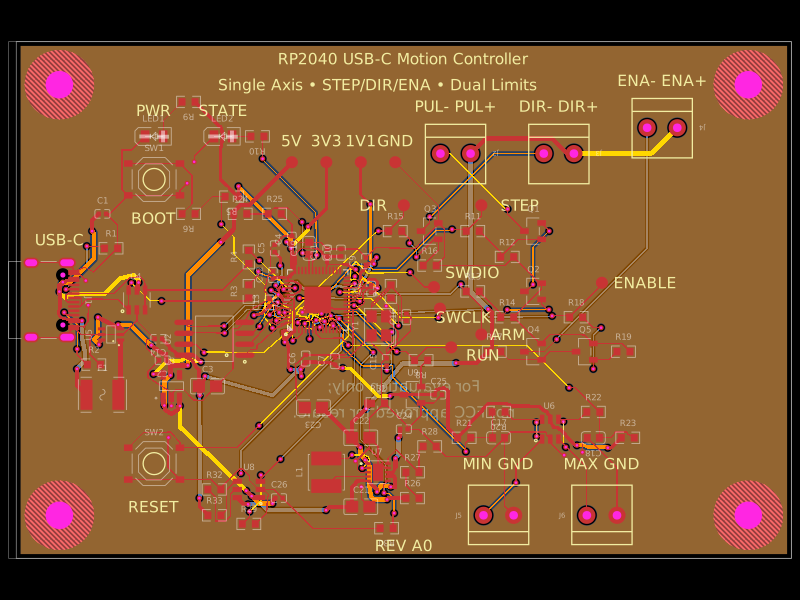 More from this authorAnasSarkiz/rp2040-usb-c-single-axis-dm542t-motion-controller--01a0e89cA USB‑C RP2040 controller board with external QSPI flash, crystal clock, regulated 3.3/1.1/5 V power, boost-converted motor-driver supply, protected USB and limit inputs, status LEDs, reset/boot switches, and AO3400A MOSFET outputs for stepper-control signals.
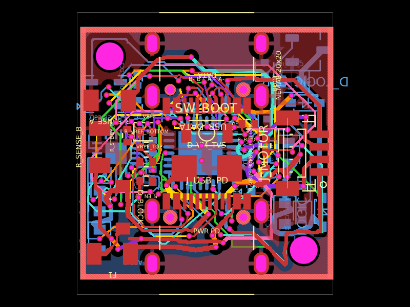 Similar packageShiboSoftwareDev/nema8-20mm-dual-usbc-stepper-controllerBAT54C is a compact three-pin SMD dual Schottky diode, while BAT54WS is a two-pin SMD single Schottky diode, each with defined PCB footprints and 3D models.
 Discover something newpixalynx/usb3-hub-10gA USB 3.2 Gen 2 six-port hub board with USB-C PD power input, regulated 5 V/3.3 V/1.15 V rails, one upstream and four protected downstream USB-A/USB-C ports, SuperSpeed muxes, ESD protection, and controlled port power.