AnasSarkiz/usb-c-pwm-pa25
A component library defining an AO3400A N-channel MOSFET, 47 µF polarized capacitor, 3-pin through-hole connector, and 9.1 V Zener diode with PCB footprints and 3D CAD models.
- Version
- 0.1.0-prototype.2
- License
- unset
- Stars
- 0
imports/TPS70933DBVR.tsx
import type { ChipProps } from "@tscircuit/props";

const pinLabels = {
	pin1: ["IN"],
	pin2: ["GND"],
	pin3: ["EN"],
	pin4: ["NC"],
	pin5: ["OUT"],
} as const;

const pinAttributes = {
	pin2: {
		requiresGround: true,
	},
	pin4: {
		doNotConnect: true,
	},
	pin1: {
		requiresPower: true,
	},
	pin3: {
		isInput: true,
	},
	pin5: {
		providesPower: true,
	},
} as const;

export const TPS70933DBVR = (props: ChipProps<typeof pinLabels>) => {
	return (
		<chip
			pinLabels={pinLabels}
			pinAttributes={pinAttributes}
			supplierPartNumbers={{
				jlcpcb: ["C89347"],
			}}
			manufacturerPartNumber="TPS70933DBVR"
			footprint={
				<footprint>
					<smtpad
						portHints={["pin5"]}
						pcbX="-1.300099mm"
						pcbY="-0.94996mm"
						width="1.0999978mm"
						height="0.5999988mm"
						shape="rect"
					/>
					<smtpad
						portHints={["pin4"]}
						pcbX="-1.300099mm"
						pcbY="0.94996mm"
						width="1.0999978mm"
						height="0.5999988mm"
						shape="rect"
					/>
					<smtpad
						portHints={["pin3"]}
						pcbX="1.300099mm"
						pcbY="0.94996mm"
						width="1.0999978mm"
						height="0.5999988mm"
						shape="rect"
					/>
					<smtpad
						portHints={["pin2"]}
						pcbX="1.300099mm"
						pcbY="-0mm"
						width="1.0999978mm"
						height="0.5999988mm"
						shape="rect"
					/>
					<smtpad
						portHints={["pin1"]}
						pcbX="1.300099mm"
						pcbY="-0.94996mm"
						width="1.0999978mm"
						height="0.5999988mm"
						shape="rect"
					/>
					<silkscreenpath
						route={[
							{ x: 0.8999728000000005, y: -1.404111999999941 },
							{ x: 0.8999728000000005, y: -1.5500604000000067 },
						]}
					/>
					<silkscreenpath
						route={[
							{ x: 0.8999728000000005, y: -0.45412660000010874 },
							{ x: 0.8999728000000005, y: -0.4958079999998972 },
						]}
					/>
					<silkscreenpath
						route={[
							{ x: 0.8999728000000005, y: 0.4958079999998972 },
							{ x: 0.8999728000000005, y: 0.45415200000002187 },
						]}
					/>
					<silkscreenpath
						route={[
							{ x: 0.8999728000000005, y: 1.5499587999998994 },
							{ x: 0.8999728000000005, y: 1.404111999999941 },
						]}
					/>
					<silkscreenpath
						route={[
							{ x: -0.9000489999999672, y: -1.404111999999941 },
							{ x: -0.9000489999999672, y: -1.5500604000000067 },
						]}
					/>
					<silkscreenpath
						route={[
							{ x: -0.9000489999999672, y: 0.4958079999998972 },
							{ x: -0.9000489999999672, y: -0.4958334000000377 },
						]}
					/>
					<silkscreenpath
						route={[
							{ x: -0.9000489999999672, y: 1.5499587999998994 },
							{ x: -0.9000489999999672, y: 1.4040866000000278 },
						]}
					/>
					<silkscreenpath
						route={[
							{ x: -0.9000489999999672, y: 1.5499587999998994 },
							{ x: 0.8999728000000005, y: 1.5499587999998994 },
						]}
					/>
					<silkscreenpath
						route={[
							{ x: -0.9000489999999672, y: -1.5500604000000067 },
							{ x: 0.8999728000000005, y: -1.5500604000000067 },
						]}
					/>
					<silkscreentext
						text="{NAME}"
						pcbX="0.012319mm"
						pcbY="2.562354mm"
						anchorAlignment="center"
						fontSize="1mm"
					/>
					<courtyardoutline
						outline={[
							{ x: -2.091880999999944, y: 1.8123540000000276 },
							{ x: 2.1165190000000393, y: 1.8123540000000276 },
							{ x: 2.1165190000000393, y: -1.786446000000069 },
							{ x: -2.091880999999944, y: -1.786446000000069 },
							{ x: -2.091880999999944, y: 1.8123540000000276 },
						]}
					/>
				</footprint>
			}
			cadModel={{
				objUrl:
					"https://modelcdn.tscircuit.com/easyeda_models/assets/C89347.obj?uuid=460193f9bf2d42e58cf3c2f675b07dc6",
				stepUrl:
					"https://modelcdn.tscircuit.com/easyeda_models/assets/C89347.step?uuid=460193f9bf2d42e58cf3c2f675b07dc6",
				pcbRotationOffset: 180,
				modelOriginPosition: {
					x: 0,
					y: -0.000012700000070253736,
					z: -0.049083,
				},
			}}
			{...props}
		/>
	);
};
Related Packages
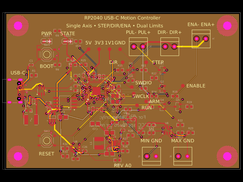 More from this authorAnasSarkiz/rp2040-usb-c-single-axis-dm542t-motion-controller--01a0e89cA USB‑C RP2040 controller board with external QSPI flash, crystal clock, regulated 3.3/1.1/5 V power, boost-converted motor-driver supply, protected USB and limit inputs, status LEDs, reset/boot switches, and AO3400A MOSFET outputs for stepper-control signals.
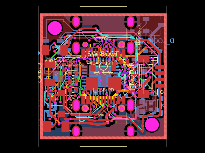 Similar packageShiboSoftwareDev/nema8-20mm-dual-usbc-stepper-controllerBAT54C is a compact three-pin SMD dual Schottky diode, while BAT54WS is a two-pin SMD single Schottky diode, each with defined PCB footprints and 3D models.
 Discover something newpixalynx/usb3-hub-10gA USB 3.2 Gen 2 six-port hub board with USB-C PD power input, regulated 5 V/3.3 V/1.15 V rails, one upstream and four protected downstream USB-A/USB-C ports, SuperSpeed muxes, ESD protection, and controlled port power.