AnasSarkiz/usb-c-pwm-pa25
A component library defining an AO3400A N-channel MOSFET, 47 µF polarized capacitor, 3-pin through-hole connector, and 9.1 V Zener diode with PCB footprints and 3D CAD models.
- Version
- 0.1.0-prototype.2
- License
- unset
- Stars
- 0
docs/TOOLING_BLOCKERS.md
# Native validation blockers — A1, 2026-09-30

This is a local reproduction record, not a submitted upstream issue. No external message or publication was sent. The project remains an unvalidated prototype; fixing a tool does not by itself approve the resulting hardware.

## Reproduction

From this board directory, install the frozen lockfile, then run:

```sh
bun install --frozen-lockfile
bunx tsci build index.circuit.tsx --pcb-png --pcb-svgs --schematic-svgs
bun test
bunx tsci check shorts dist/index/circuit.json
bunx tsci snapshot index.circuit.tsx
```

Pinned versions: tscircuit 0.0.2679, CLI 0.1.2193, core 0.0.2016, runframe 0.0.2848, capacity-autorouter 0.0.941, circuit-json 0.0.506, Bun 1.3.9. Routing is enabled, pipeline 7, 2x effort, local, four layers, ordinary full-stack vias, 3,600,000 ms worker timeout. There are no imported routing arrays.

The default four-layer build emits 301 traces and 204 vias, returns zero and contains no native error records, while its log contains:

```text
Async effect error in PcbDesignRuleChecks "board:drc-checks":
Error: source_net_36_mst1_0: Unresolved boundary conflict in boolean operation
```

The stack begins at `convertCircuitJsonToFlattenJs`, then `checkCopperPourShorts`, then `runAllRoutingChecks`. The snapshot command repeats the exception, writes snapshots and says they match. Both results are rejected. Expected behavior is a surfaced failing status and a completed, reliable DRC result before acceptance.

Independent checks find:

- One Gerber-level top short at (-26.135, 2.012) mm: U1.DRAIN2 to CC2. The pin is intentionally unconnected; copper must still avoid it.
- Fifteen ordinary drill-to-solder-pad pairs below 0.20 mm, including actual overlaps at R41 and U1. This happens with `allowViaInPad: false`, 0.60/0.30 mm vias and 0.30 mm configured via-edge-to-pad clearance. Same-net pads also need drill protection.
- Twenty-three emitted wire-point width values below the configured 0.15 mm minimum; the smallest is 0.10 mm.

Evidence: `evidence/routed-four-layer-rejected/circuit.json`, `shorts-a1-four-layer.log`, `via-pad-clearance-a1-four-layer.json`, `trace-widths-a1-four-layer.json`, `board-tests-routed-a1-final.log`, `snapshot-a1-four-layer.log`. Four native layer previews are under `output/pcb-review`; all are explicitly rejected. Snapshot files are retained in `evidence/rejected-snapshots` and are not accepted baselines.

## Congestion analysis

`bunx tsci check routing-difficulty evidence/unrouted-a1-four-layer/circuit.json` produces no output while consuming one CPU core. Earlier two-layer source and JSON attempts also stalled for 16–44 minutes. The task-owned stalled processes were explicitly stopped; the 60-minute build-worker setting was not changed. There is no congestion-check pass.

The official command delegates to `analyzeRouting`. Inspection of the bundled analysis found a solver-phase wait loop that depends on reaching `highDensityRouteSolver` and does not visibly check the solver's failed/solved state inside that loop. This is a diagnosis to confirm upstream, not a proven universal cause. The saved command source is `evidence/official-routing-difficulty.ts.txt`. Fix the canonical tool and rerun it; a custom diagnostic is not an accepted replacement.

## Supplier rotations

`circuit-json-to-pnp-csv` 0.0.16 with supplier `jlcpcb` and `requireSupplierRotation: true` rejects U2 for missing authored pin-1 location. Diagnostic enumeration finds the same for U5, J3, J4, D3, D4 and D5, plus missing supplier metadata for C19. See `evidence/cpl-orientation-unresolved.json`. Resolve native footprint/orientation metadata and review the actual supplier placement preview before approving a CPL. Do not silently use unverified PCB rotations.

## Next acceptance attempt

Retain these independent regression checks. Repair the native tooling, regenerate copper from declarative source, and require completed DRC, no shorts, valid widths and all ordinary drills clear of every solder pad. Reinspect power paths, return paths, converter loops, all four layers and mechanical clearances. Then generate and review the fabrication set and supplier assembly orientation from the same manifested revision. Physical prototype tests remain a later, separate gate.
Related Packages
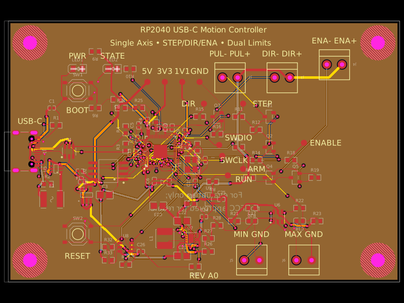 More from this authorAnasSarkiz/rp2040-usb-c-single-axis-dm542t-motion-controller--01a0e89cA USB‑C RP2040 controller board with external QSPI flash, crystal clock, regulated 3.3/1.1/5 V power, boost-converted motor-driver supply, protected USB and limit inputs, status LEDs, reset/boot switches, and AO3400A MOSFET outputs for stepper-control signals.
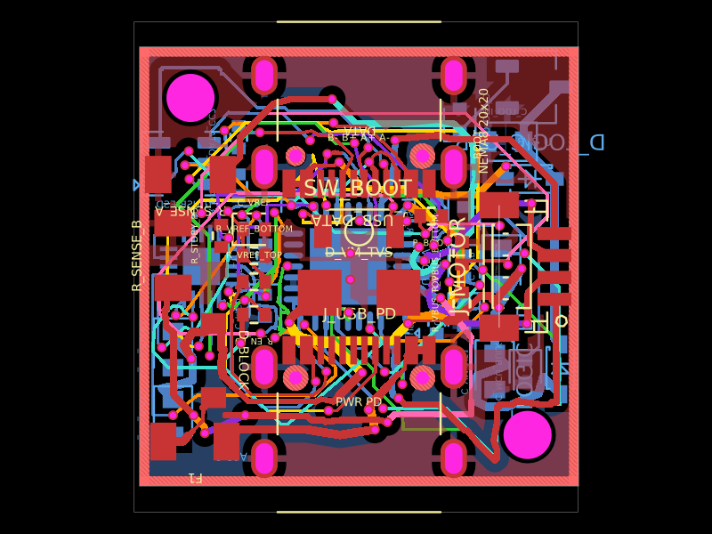 Similar packageShiboSoftwareDev/nema8-20mm-dual-usbc-stepper-controllerBAT54C is a compact three-pin SMD dual Schottky diode, while BAT54WS is a two-pin SMD single Schottky diode, each with defined PCB footprints and 3D models.
 Discover something newpixalynx/usb3-hub-10gA USB 3.2 Gen 2 six-port hub board with USB-C PD power input, regulated 5 V/3.3 V/1.15 V rails, one upstream and four protected downstream USB-A/USB-C ports, SuperSpeed muxes, ESD protection, and controlled port power.