AnasSarkiz/usb-c-pwm-pa25
A component library defining an AO3400A N-channel MOSFET, 47 µF polarized capacitor, 3-pin through-hole connector, and 9.1 V Zener diode with PCB footprints and 3D CAD models.
- Version
- 0.1.0-prototype.2
- License
- unset
- Stars
- 0
docs/MECHANICAL.md
# A1 mechanics and assembly

The board is 90 × 65 mm, four copper layers, 1.6 mm FR-4, specified 1 oz copper on all layers, green mask and lead-free HASL or ENIG. The brief permits four layers; this revision uses them after two-layer native routing failed independent shorts and drill-clearance checks. This does not establish that a two-layer design is impossible. JLCPCB's [stackup selector](https://jlcpcb.com/impedance), checked 2026-09-30, offers 1 oz inner copper; explicitly select that option rather than the default 0.5 oz. Order is top / inner1 / inner2 / bottom, all available to native routing with GND pours. No controlled impedance is specified. Obtain the manufacturer's exact dielectric stack and finished copper/plating tolerances before fabrication approval.

Dimensions were selected from the actual footprints and connector access, not the absent reference photo. Four 3.2 mm non-plated mounting holes have centers at (±40, ±27.5) mm relative to board center: an 80 × 55 mm mounting pattern. Each has a 4 mm radius copper keepout on all four layers. Use insulated M3 standoffs and washers no larger than the keepout diameter.

USB enters from the left. The motor terminal is at the right. Two top-edge JST PH connectors serve panel controls. Programming is accessible from the lower edge. Leave a clear approach for each mating connector and cable bend; do not clamp the USB plug against the enclosure wall. The GCT USB4105 shell stakes provide retention; the enclosure must also strain-relieve the external cable. The motor wires need separate strain relief and must not pull on J2.

Maximum component height is set by the selected bulk/output capacitors and terminal. Reserve at least 16 mm above the board and 3 mm below it for the initial ventilated enclosure; confirm against the final component drawings and physical sample before making enclosure tooling. The hot braking-resistor area is along the upper-right edge and must remain clear of cables and plastic. No sealed-enclosure or continuous back-driving rating is assigned.

## Panel hardware

Use Bourns PDB181-K420K-103B: 10 kΩ linear, no detents, 20 mm long 6 mm / 18-tooth knurled shaft, M7 × 0.75 threaded panel bushing; nut and washer are supplied. Use a compatible 6 mm / 18-tooth knob. Its PC pins may be wired with insulated, strain-relieved leads for the prototype; the threaded bushing carries the mechanical load. Pin 2 is wiper; verify the clockwise end with a meter before connecting J3. Reserve room for the 17 mm body and lead insulation behind the panel. Final knob/enclosure fit is a physical mechanical test.

Use C&K 7103SYZBE: maintained SPDT ON-OFF-ON, 10.67 mm toggle, 8.89 mm threaded 1/4-40 bushing, solder lugs and gold dry-circuit contacts. This suits approximately 0.33 mA at 3.3 V. Common lug 2 goes to J4 pin 2; wire the outer contacts so the visible FWD position closes J4 pins 1–2. Verify orientation with a meter; do not infer it from the lever alone. Use the supplied nut/locking hardware and insulate solder lugs. Panel controls and knob are separately procured, not PCB-assembly line items.

Each control lead uses a JST PHR-3 housing with three SPH-002T-P0.5S contacts for suitable 24–28 AWG wire; check JST's exact wire/insulation limits and use the specified crimp tool. Keep leads ≤150 mm inside the enclosure. J5 mates to PHR-5 with the same contact family. The motor pair is 22–24 AWG twisted wire, initially ≤300 mm. Do not combine motor-current return with a control-cable ground.

## Fabrication rules

Target JLCPCB standard rigid-board capabilities, checked 2026-09-30: use ≥0.15 mm signal traces/clearance; ≥0.60 mm via pads with ≥0.30 mm drills (0.15 mm nominal annular ring); ≥0.25 mm drill-to-drill gap; ≥0.20 mm via copper-edge-to-pad clearance; ≥0.50 mm copper-to-board-edge clearance. Mounting keepouts are wider. Ordinary tented through vias only; no blind/buried vias or ordinary drilled vias within solder pads. Require a documented finished via-barrel plating thickness for the power-via calculation. A manufacturer DFM response is still required before fabrication approval.

Native routing targets 0.8 mm main power/motor connections, with separately reviewed package neck-downs. All four layers carry GND pours; their continuity and power-return paths must be reviewed on actual output. U6 has four external thermal vias; its exposed pad must be soldered. Do not restore the imported ordinary in-pad drill pattern.

## Assembly sequence

1. Inspect the final Gerber/drill/mask/paste set and confirm it matches the validated revision and checksums.
2. Review CPL orientation against the native assembly preview and JLCPCB's actual placement preview. Confirm pin 1 on U1/U2/U5/U6/U9, LED/zener polarity, and the positive marks on polarized capacitors. BOM and CPL reference sets must match the parts selected for the assembly service.
3. SMT-assemble the ICs, passives, LEDs, USB connector and SWD connector. Verify exposed-pad soldering and QFN joints, preferably by X-ray. J1 shell stakes require through-hole soldering compatible with the selected process.
4. Hand-solder separately procured C15 (positive pad 1 to V12_BUCK), and J2/J3/J4 or arrange a separate through-hole service. Fit panel hardware and crimped harnesses after board inspection. Do not include holes, test pads or fiducials as purchased components.
5. With the motor disconnected, program and verify the firmware and brownout option bytes per `firmware/README.md`.
6. Execute the prototype test plan. Record measured results, including thermal and mechanical evidence, before assigning application limits.

The reference supply is a 30 W USB-C PD charger offering fixed 15 V / 2 A (Anker A2147 was checked as a candidate). Use a known-compliant USB-C to USB-C 3 A cable ≤1 m. No USB-A or ordinary computer-port motor operation is supported. Regional charger label, cable SKU and physical procurement checks belong in the actual test record.
Related Packages
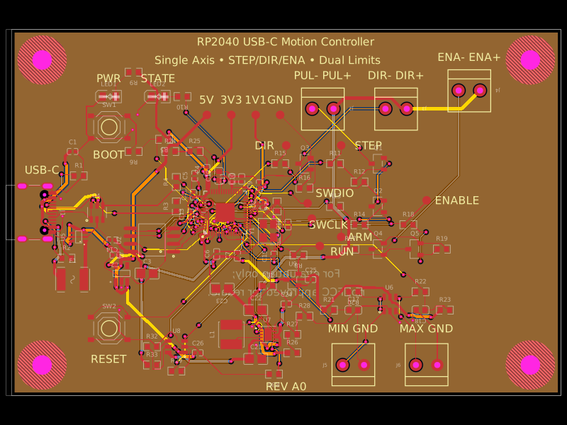 More from this authorAnasSarkiz/rp2040-usb-c-single-axis-dm542t-motion-controller--01a0e89cA USB‑C RP2040 controller board with external QSPI flash, crystal clock, regulated 3.3/1.1/5 V power, boost-converted motor-driver supply, protected USB and limit inputs, status LEDs, reset/boot switches, and AO3400A MOSFET outputs for stepper-control signals.
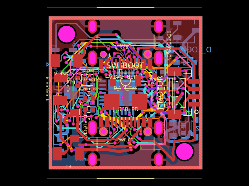 Similar packageShiboSoftwareDev/nema8-20mm-dual-usbc-stepper-controllerBAT54C is a compact three-pin SMD dual Schottky diode, while BAT54WS is a two-pin SMD single Schottky diode, each with defined PCB footprints and 3D models.
 Discover something newpixalynx/usb3-hub-10gA USB 3.2 Gen 2 six-port hub board with USB-C PD power input, regulated 5 V/3.3 V/1.15 V rails, one upstream and four protected downstream USB-A/USB-C ports, SuperSpeed muxes, ESD protection, and controlled port power.