AnasSarkiz/usb-c-pwm-pa25
A component library defining an AO3400A N-channel MOSFET, 47 µF polarized capacitor, 3-pin through-hole connector, and 9.1 V Zener diode with PCB footprints and 3D CAD models.
- Version
- 0.1.0-prototype.2
- License
- unset
- Stars
- 0
docs/CALCULATIONS.md
# A1 calculations and intended bench limits

Revision A1, 2026-09-30. These are design calculations, not measured performance. Manufacturer references are registered in `references/README.md`.

## Motor and current regulation

The PA25-24126000-G23 drawing specifies 12 V, 250 mA rated current, 20 mA no-load current, 199/266 rpm geared rated/no-load speeds, 0.54 kg·cm rated geared torque and 22.56:1 ratio. Rated electrical input is 3 W. The separate 1.4 W entry is not electrical consumption. Torque × speed gives about 1.10 W geared output; the drawing does not reconcile these two mechanical figures. Starting/stall current, winding thermal limits and safe stall duration remain measurements to obtain.

DRV8874 uses 450 µA/A nominal IPROPI scaling. R30 || R31 = 10 kΩ || 820 kΩ = 9.8795 kΩ. With the LM4040 2.5 V reference, Itrip = 2.5/(9879.5 × 450e-6) = **0.5623 A**. Using ±7.5% scaling at 0.4–1 A, ±1% resistance, and a ±0.5% reference design allowance gives approximately **0.515–0.617 A**. The selected B-grade reference has ±0.2% initial tolerance; the wider allowance includes temperature/load effects over the intended 0–40 °C bench ambient. Dynamic overshoot, blanking and comparator delays are additional; reserve 0.65 A for budgeting and measure peaks. This is never a continuous motor rating.

At lower currents the driver specifies ±30 mA sensing error, before external and ADC errors. Firmware latches a fault when measured current is at least 350 mA for 100 ms. This verifies sustained-overload handling but cannot establish a safe intentional stall time. No locked-rotor test is authorized by this calculation. PWM is 12 MHz / 600 = 20 kHz; 2 permille/ms ramp steps take 500 ms from zero to full command.

## Regulated rail and PD budget

TPS54202 uses R16=191 kΩ and R17=10 kΩ: 0.596 × (1+19.1) = **11.9796 V**. Combining the 0.581–0.611 V feedback limits with independent 1% resistors gives **11.458–12.517 V** before load/line drops. Firmware accepts measured VM from 11.1 to 12.8 V; verify measurement error and transients physically. A typical 12 V label does not imply ±2% regulation.

Budget: output voltage 12.517 V; motor-path current 0.65 A; other 12 V current 0.02 A; minimum efficiency target 85%; input-side control/protection allowance 0.35 W; margin 25%.

Pinput = ((12.517 × 0.67)/0.85 + 0.35) × 1.25 = **12.77 W**. This is 0.851 A at 15 V and 0.946 A at the conservative 13.5 V board-input analysis point. The latter is an analysis point, not a USB-PD specification. U1 requests **1 A operating / 1.5 A maximum** at fixed 15 V. Firmware requires the actual source PDO to offer at least 1.5 A and verifies the active request. Reference supply: 30 W USB-C PD with fixed 15 V/2 A, a compliant 3 A C-to-C cable no longer than 1 m. No 12 V PDO, USB-A adapter or ordinary computer port is relied upon.

TPS259470L ILM=2.8 kΩ gives about 1.19 A, with approximately ±10% IC tolerance above 1 A plus resistor tolerance (about 1.06–1.33 A). This sits below the requested 1.5 A maximum. Initial bulk charge at 0.2 V/ms into 470 µF requires 94 mA plus load; firmware inhibits the bridge through settling. Both eFuses have 10 nF dVdt capacitors and latched fast-trip configuration. Q2/Q3 reset both paths. Nominal UV/OV thresholds: U2 13.2/16.8 V; U5 10.872/13.2 V. Threshold and resistor tolerances must be included in supply corner tests.

## Buck energy storage and compensation

L1 is Bourns SRP7050TA-150M: 15 µH ±20%, 3.5 A RMS, 6 A saturation, 92 mΩ maximum DCR. Nominal inductor ripple at 15 V → 12 V, 500 kHz is 0.32 A peak-to-peak. A conservative 16.8 V, 12 µH, 400 kHz corner gives 0.714 A peak-to-peak: approximately 1.007 A peak at the 0.65 A motor budget. The 6 A saturation rating also accommodates the regulator's much higher internal short-circuit peak-current threshold; it does not make this a 6 A board.

C15 is **Panasonic 25SVPF47M**, 47 µF ±20%, 25 V polymer, 30 mΩ maximum initial ESR, 2.8 A ripple rating. C16 is 100 nF ceramic. The polymer avoids using unverified MLCC DC-bias capacitance as the regulator's bulk output. Initial minimum is 37.6 µF; including the datasheet's 20% endurance change gives 30.08 µF. These are not a lifetime prediction. At 0.714 A ripple, capacitor RMS current is about 0.206 A. The estimated capacitive ripple at 400 kHz and 30.08 µF is 7.4 mV; initial ESR adds about 21.4 mV. Endurance ESR and temperature require measurement.

TI's small-ESR crossover estimate, 3.95/(Vout × Cout), gives 7.02 kHz nominal and 10.96 kHz at the above minimum, below its 40 kHz guidance. The ideal small-ESR feed-forward value is about 119 pF; TI instructs reducing it for medium ESR. C19=47 pF gives a zero at about 17.7 kHz with 191 kΩ. This is a starting compensation choice, not a measured phase margin. Bench acceptance requires stable startup, line/load steps and no sustained ringing; measure the loop if needed. The 500 kHz input bypass loop and SW area must be assessed on actual routed copper.

## Regeneration and thermal shutdown

The downstream reverse-blocking U5 prevents VM feeding the buck or USB source. A 470 µF capacitor alone stores only 12.22 mJ between 12 and 14 V. U7/U8 are powered from VM so the dissipative clamp can operate after USB removal.

R41=43.2 kΩ, R42=10 kΩ and R43=820 kΩ with a 2.5 V reference give about **13.432 V turn-on** at a low comparator output. With the gate limited near 9.1 V by D6, turn-off is about **12.95 V**. Component tolerances, comparator offset, output low voltage and zener operating current change these values. Target peak VM <14 V in initial bench tests; this is an acceptance target, not a guaranteed transient bound.

R70–R77 are eight Bourns CRM2512AJW-201ELF, 200 Ω ±5%, 2 W pulse-resistant parts in parallel: 25 Ω nominal. At 14 V the bank draws 0.56 A and dissipates 7.84 W, or 0.98 W each. The initial **≤0.5 J/event and ≤1 W average** test envelope is deliberately limited; 0.5 J corresponds to about 64 ms at 14 V. The CRM-A pulse curve provides substantial pulse headroom at this duration, but does not qualify the board's continuous thermal performance. No 16 W continuous board rating is claimed. Q1 switches this load with a protected gate; its transient safe operating area and temperature still need scope/thermal verification.

The 10 kΩ/B3380 NTC with a 27.4 kΩ pull-up gives a nominal hardware trip around 70 °C against the 0.250 V comparator threshold. Firmware trips earlier at 300 mV (about 65 °C) and treats >1.8 V as an open-sensor fault. Actual temperatures depend on tolerance and sensor placement. Board temperature does not represent winding temperature.

STOP or a direction change ramps PWM down, enters coast, waits at least 2 s, and requires deliberate STOP/zero re-arming. There is no speed sensor: the 2 s interval does not prove the shaft has stopped. Characterize stopping time for the actual mechanism before loaded use. External back-driving, suspended loads and continuous regeneration are outside this bench prototype's assigned scope.

## Copper basis and remaining measurements

Use four layers with specified 1 oz copper on every layer, 0.8 mm main power/motor routes where possible, ≥0.15 mm signals/clearance, 0.60/0.30 mm ordinary tented through vias, ≥0.5 mm edge clearance and 4 mm-radius mounting keepouts. Nominal copper resistivity at 20 °C is 1.724e-8 Ω·m: a 0.8 mm × 35 µm trace is about 0.616 mΩ/mm; at 0.65 A a 50 mm path loses about 20 mV and 13 mW. A 0.15 mm × 35 µm neck is 3.284 mΩ/mm; a 2 mm neck loses about 4.27 mV and 2.78 mW at 0.65 A. These electrical losses are not a thermal model or permission for arbitrarily long narrow power routes. Inner-layer thermal behavior must be reviewed separately; an external-layer ampacity assumption cannot be applied to an internal trace. The 1 oz inner-copper option is a fabrication requirement, not the default 0.5 oz stack.

For a 0.30 mm drill and assumed 20 µm finished plating, a 1.6 mm barrel is about 1.46 mΩ (0.62 mW at 0.65 A). Manufacturer-confirmed plating and actual via count are required. Ground pours, package escapes, physical neck lengths, drill/pad gaps and all power transitions must be measured from the routed output. Physical thermals remain pending. Configuration values alone do not pass copper validation.
Related Packages
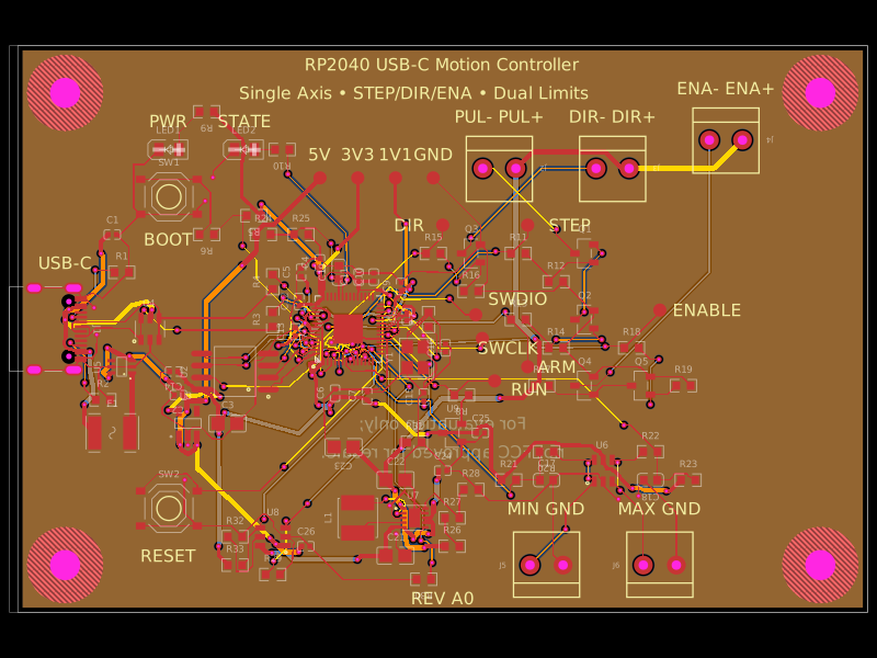 More from this authorAnasSarkiz/rp2040-usb-c-single-axis-dm542t-motion-controller--01a0e89cA USB‑C RP2040 controller board with external QSPI flash, crystal clock, regulated 3.3/1.1/5 V power, boost-converted motor-driver supply, protected USB and limit inputs, status LEDs, reset/boot switches, and AO3400A MOSFET outputs for stepper-control signals.
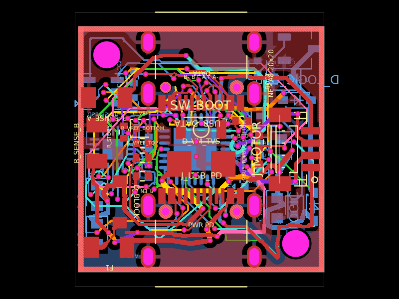 Similar packageShiboSoftwareDev/nema8-20mm-dual-usbc-stepper-controllerBAT54C is a compact three-pin SMD dual Schottky diode, while BAT54WS is a two-pin SMD single Schottky diode, each with defined PCB footprints and 3D models.
 Discover something newpixalynx/usb3-hub-10gA USB 3.2 Gen 2 six-port hub board with USB-C PD power input, regulated 5 V/3.3 V/1.15 V rails, one upstream and four protected downstream USB-A/USB-C ports, SuperSpeed muxes, ESD protection, and controlled port power.