AnasSarkiz/usb-c-pwm-pa25
A component library defining an AO3400A N-channel MOSFET, 47 µF polarized capacitor, 3-pin through-hole connector, and 9.1 V Zener diode with PCB footprints and 3D CAD models.
- Version
- 0.1.0-prototype.2
- License
- unset
- Stars
- 0
docs/ARCHITECTURE.md
# A1 architecture and schematic review

Date: 2026-09-30. Circuit entry: `index.circuit.tsx`; six native A4 sheets in `lib/`. This is a new design, not an inherited motor-mounted controller.

## Power and control

J1 → TPS25730D PD sink → TPS259470L protected 15 V path → TPS54202 12 V buck → TPS259470L reverse blocker → DRV8874 → J2. TPS709 supplies 3.3 V control power from PD_OUT, including before 15 V negotiation. VM has a 470 µF capacitor and an independent LM393B-controlled 25 Ω dissipative clamp.

The standalone PD controller uses hardware straps, with no NVM image. It can still pass default 5 V: strap settings alone do not prove a 15 V contract. The STM32 reads its active PDO/RDO over I2C and independently releases the input eFuse; an analog 13.2 V UV threshold rejects default 5 V. This qualification, restart latch, sustained-overload timing and reversal sequence justify the small MCU instead of a larger collection of timers, comparators and flip-flops. The hardware bridge-current limit and HEALTH interlock remain independent of firmware.

## Pin / configuration review

The following connections were reviewed against the local manufacturer PDFs, with current supplier identity records in `evidence/catalog/`.

| Circuit | Reviewed behavior and connections |
|---|---|
| J1 / D1 / D2 | GCT USB4105 mechanically retained by four shell stakes. All VBUS contacts joined, all ground/shield contacts joined. CC1/CC2 separate into U1; no duplicate Rd resistors. USB data/SBU pins NC. TVS2200 on VBUS; TPD2E2U06 only on CC. 330 pF CC shunts. |
| U1 TPS25730DREFR | ADCIN codes 3/5/1/0 request 15 V minimum/maximum, 1 A operating and 1.5 A maximum, address 0x21. All VBUS/PPHV and ground pins included; reserved pins grounded. VIN_3V3 grounded for dead-battery operation. LDO outputs each decoupled by 10 µF. FAULT_IN high. DRAIN pads intentionally NC per reference guidance, unused status outputs NC. |
| U2 / U5 TPS259470LRPWR | Exact latched variant with continuous reverse blocking. IN/OUT direction correct; UV/OV dividers, 2.8 kΩ ILM and 10 nF dVdt. ITIMER floating chooses fast trip. AUXOFF and FLT are open drain on HEALTH. Q2/Q3 share the default-high power-inhibit signal and reset both stages. |
| U3 TPS70933DBVR | Input on PD_OUT, output 3.3 V; 1 µF input and 4.7 µF output. EN floating is explicitly enabled; NC pin unused. 30 V input rating. |
| U4 TPS54202DDCR | 15 V → nominal 11.98 V. Pin 1 GND, 2 SW, 3 VIN, 4 FB, 5 EN, 6 BOOT. EN internally pulled up and left NC. 191 kΩ / 10 kΩ feedback, bootstrap 100 nF and feed-forward capacitor. L1 is shielded 15 µH, 6 A saturation rating. |
| U6 DRV8874PWPR | VM is regulated and reverse-blocked, not raw VBUS. PMODE=GND selects PH/EN. IMODE floating selects 25 µs off-time and latched OCP. PH high drives OUT1 positive. EN low brakes; nSLEEP low coasts. CPH/CPL 22 nF, VCP/VM 100 nF, local VM 100 nF plus bulk. IPROPI 10 kΩ || 820 kΩ and separate ADC filter. PGND/GND/EP all ground. |
| U7 LM4040B25IDBZR | 2.5 V shunt reference biased from VM, so the clamp persists after USB removal. Cathode is reference, anode ground, pin 3 grounded as permitted. 4.7 kΩ bias supplies approximately 2 mA. |
| U8 LM393BIDR / Q1 / D6 | Channel A drives the clamp MOSFET gate through an open-collector output and pull-up. A 9.1 V zener protects the ±12 V gate. Positive feedback gives hysteresis. Channel B compares NTC voltage with approximately 0.25 V and pulls HEALTH low on excess temperature. |
| U9 STM32C011F4P6 | VDD/VSS, NRST, all selected GPIO functions and TSSOP20 pin numbering cross-checked with ST. PA4 AF4 is TIM14; PB6/PB7 AF6 are I2C1. PA11/PA12 use default mapping. VREFINT channel 10 and factory calibration address 0x1FFF756A verified against ST's LL header. |
| U10 SN74LVC1G08DBVR | Hardware AND of MCU_ENABLE and HEALTH drives nSLEEP. 100 kΩ pulldowns hold MCU enable, nSLEEP and PWM inactive at reset. |
| J5 | Five-pin JST PH standard matches the official tscircuit biscuit-board example. Mechanical tabs are NC. |

The native pin checker reports six chip-wrapper warnings for D1/D2, Q1/Q2/Q3 and U7 having no `requiresPower` pin. These are passive protection parts, MOSFETs and a shunt reference, not conventional powered logic ICs. Their actual pins are specified and connected correctly. Do not add a fictitious VCC pin to silence this warning.

## Footprints and assembly

Exact imported supplier footprints are in `imports/`; generic passives use explicit package sizes and manufacturer/supplier identities. U6's imported ordinary in-pad vias were removed. Four 0.60/0.30 mm ground vias now sit outside its exposed pad. The Bourns L1 land pattern was corrected after visually reviewing its official drawing: 8.4 mm total width, 2.5 mm gap, 3.5 mm pad height. LED and zener polarity were checked from their source pad numbering. Connector pin order, keepouts and entry directions are part of placement review.

Supplier rotation metadata is fetched by the native parts engine. CPL must use that metadata and be checked against an assembly preview; an imported footprint alone does not certify an assembler's rotation. Through-hole J2/J3/J4 and J1's shell stakes require the appropriate assembly process. No part substitutes have been qualified.

## Deliberate limits

The initial build targets an unloaded, supervised motor test. The final mechanism, back-driving energy and reversal duty are unknown; they are not assigned an invented rating. Normal control, brownout and cable-removal behavior have separate bench tests. Input surge/ESD immunity, buck loop stability, motor winding limits and braking heat remain physical qualification items. No FCC compliance or tested-hardware claim is made.
Related Packages
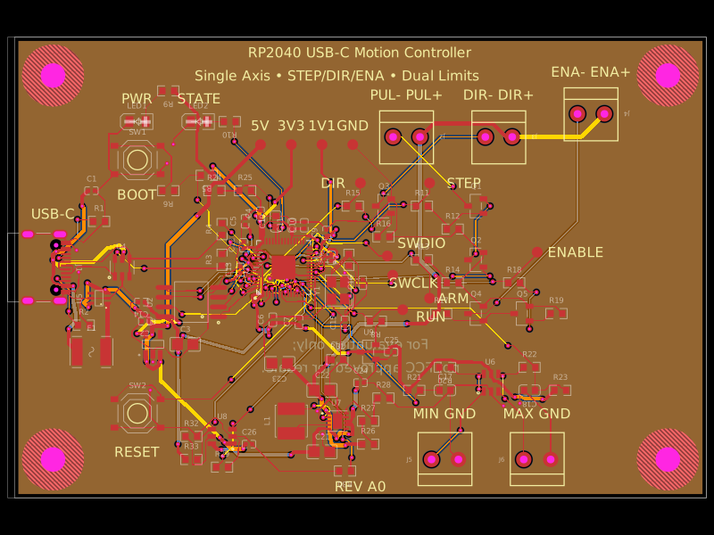 More from this authorAnasSarkiz/rp2040-usb-c-single-axis-dm542t-motion-controller--01a0e89cA USB‑C RP2040 controller board with external QSPI flash, crystal clock, regulated 3.3/1.1/5 V power, boost-converted motor-driver supply, protected USB and limit inputs, status LEDs, reset/boot switches, and AO3400A MOSFET outputs for stepper-control signals.
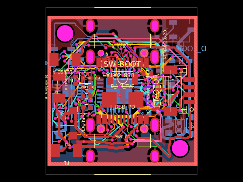 Similar packageShiboSoftwareDev/nema8-20mm-dual-usbc-stepper-controllerBAT54C is a compact three-pin SMD dual Schottky diode, while BAT54WS is a two-pin SMD single Schottky diode, each with defined PCB footprints and 3D models.
 Discover something newpixalynx/usb3-hub-10gA USB 3.2 Gen 2 six-port hub board with USB-C PD power input, regulated 5 V/3.3 V/1.15 V rails, one upstream and four protected downstream USB-A/USB-C ports, SuperSpeed muxes, ESD protection, and controlled port power.