AnasSarkiz/rp2040-usb-c-single-axis-dm542t-motion-controller--01a0e89c
A USB‑C RP2040 controller board with external QSPI flash, crystal clock, regulated 3.3/1.1/5 V power, boost-converted motor-driver supply, protected USB and limit inputs, status LEDs, reset/boot switches, and AO3400A MOSFET outputs for stepper-control signals.
- Version
- 0.1.0-prototype.19
- License
- unset
- Stars
- 0
fabrication/A0-prototype.11/README.md
# A0 / 0.1.0-prototype.11 manufacturing review package

**Untested prototype — NOT APPROVED TO ORDER OR CUT A STENCIL.**

The native `gerbers.zip` and its unchanged `exported/` contents were generated from the routed circuit identified in `manifest.json`. Copper, connectivity and dimensional checks pass. The package contains top/bottom copper, mask, paste and silk, the outline, plated/NPTH drills, the native BOM and a JLCPCB placement file. `assembly-bom.csv` is the complete authored sourcing BOM; the native BOM has matching codes but less descriptive fields.

Target construction: 90 × 60 × 1.0 mm FR-4, two copper layers, nominal 1 oz outer copper, top component assembly. All 85 fitted designators match the placement file. Placement coordinates are millimetres relative to board centre, positive X right and positive Y up; rotations are the native JLCPCB export convention. The assembler must verify component library zero orientations, polarity and connector orientation before acceptance. No assembler review has occurred.

The outline spans X ±45 mm and Y ±30 mm. Four 3.2 mm finished mounting holes are NPTH at (±40, ±25) mm. The NPTH file also contains the USB locating holes. The plated drill file contains the USB shell slots, 1.0 mm terminal holes and 0.3 mm vias. Slots use Excellon G85 commands. Copper stays at least 0.5 mm from the board edge and 4.01059 mm from mounting centres.

## Blocking stencil issue

The installed `@tscircuit/core` 0.0.1971 unconditionally generates top and bottom solder-paste circles for circular plated holes. Its public `CirclePlatedHoleProps` has no independent paste control. The ten J2–J6 terminal positions therefore have twenty unwanted paste openings, across both stencil layers. These terminals are not intended for pin-in-paste assembly. `bun run test:fabrication` intentionally fails and records this defect in `review.json`.

Paste on all eleven bare test pads has been removed through supported source properties, without changing their copper or exposed solder-mask openings. The through-hole issue requires a proper core/API fix followed by regeneration, not editing exported Gerbers or suppressing the check. The exported font also omits the two bullet glyphs in the requested subtitle; the source text is exact, but this needs an export/font fix before final silkscreen approval. Stencil aperture/reduction approval for the exposed pads and fine-pitch ICs is also pending assembler feedback.

No order has been placed. No physical board, assembly, programming, USB, loaded output or motor test has been performed.

## Reproduce

From the board directory, build the current source, then use the installed CLI's supported `export ... --format gerbers` option with `dist/index/circuit.json` and an absolute output path. Run `python3 scripts/check-fabrication.py` after extracting the native archive. `bun scripts/render-gerbers.cjs` renders the actual exported layers with the pinned gerber-to-svg 4.2.8 dependency. Full gate results are in the board's VALIDATION.md.
Related Packages
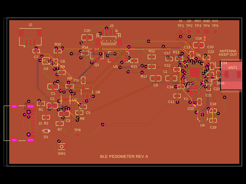 More from this authorAnasSarkiz/ble-pedometerThis code defines and configures various electronic hardware components such as surface-mount resistors, crystals, diodes, transistors, connectors, and switches with their physical footprints, schematic symbols, and 3D CAD models for PCB assembly.
 Similar packageaura/diy-power-delivery-triggerThis hardware design implements a USB Type-C port with supporting power management and signal conditioning components, including a USB-C connector, a FUSB302 USB-C port controller, ESD protection diodes, a buck converter for 3.3V power regulation, an STM32 microcontroller for control and processing, an RGB LED indicator, push button, terminal block connections, and associated filtering and support components.
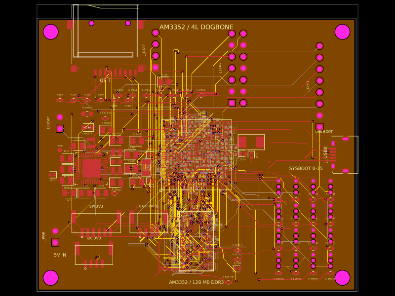 Discover something newseveibar/am3352-dev-board-4layer-dogboneDefines PCB footprints and pin mappings for a TI AM3352ZCZ100 processor, JST GH connectors, and assembly-part lookup helpers for capacitors, resistors, and headers.