AnasSarkiz/NEMA14_RP2040
A NEMA stepper motor assembly concept with a controller board, proposed M3 screws and spacers, four motor leads with insulated splices, and a JST 4-pin connector harness.
- Version
- 1.12.2
- License
- ISC
- Stars
- 0
scripts/repair-same-side-copper.py
"""Finish physically disconnected nets on exact supplier geometry.

The conservative routing grid is only a construction aid. Native DRC and the
independent physical/CAM checks are required afterward.
"""
import json, math, heapq, sys
import numpy as np
from PIL import Image,ImageDraw
from scipy.ndimage import distance_transform_edt
from shapely.ops import unary_union
import verify_supplier_connectivity as g

j=g.j;ROOT=g.ROOT;STEP=.025;LOW=-17.5;N=1401
layers=['top','bottom'] if next(e for e in j if e['type']=='pcb_board')['num_layers']==2 else ['top','inner1','inner2','bottom']
nets={e['subcircuit_connectivity_map_key']:e for e in j if e['type']=='source_net'}
traces={e['subcircuit_connectivity_map_key']:e['source_trace_id'] for e in j if e['type']=='source_trace'}
for k,name in g.nets.items():
 if k not in nets:nets[k]={'name':name,'source_net_id':None}
xy=lambda x,y:(round((x-LOW)/STEP),round((y-LOW)/STEP))
world=lambda q:(LOW+q[0]*STEP,LOW+q[1]*STEP)
def blocked(net,via=False):
    draw_layers=['top','inner1','inner2','bottom'] if via and next(e for e in j if e['type']=='pcb_board')['num_layers']==4 else layers
    images=[Image.new('L',(N,N)) for _ in draw_layers];ds=[ImageDraw.Draw(im) for im in images]
    margin=max(.15+current_via_diameter/2+.003,.30+current_via_hole/2+.003) if via else .15+current_width/2+.003
    def add(ls,geom,extra=0):
        p=geom.buffer(margin+extra,quad_segs=16)
        pieces=list(p.geoms) if hasattr(p,'geoms') else [p]
        for l in ls:
            if l not in draw_layers:continue
            d=ds[draw_layers.index(l)]
            for piece in pieces:
                if piece.geom_type=='Polygon':d.polygon([xy(x,y) for x,y in piece.exterior.coords],fill=1)
    for e in j:
        typ=e['type']
        if typ in ['pcb_smtpad','pcb_plated_hole']:
            if g.key(e)==net and not via:continue
            add(e.get('layers',[e.get('layer','top')]),g.geometry(e),-.135 if g.key(e)==net and via else 0)
        elif typ=='pcb_via':
            if g.key(e)==net and not via:continue
            add(draw_layers,g.Point(e['x'],e['y']).buffer(e['outer_diameter']/2))
        elif typ=='pcb_trace' and g.key(e)!=net:
            for a,b in zip(e['route'],e['route'][1:]):
                if a['route_type']==b['route_type']=='wire' and a['layer']==b['layer']:
                    add([a['layer']],g.LineString([(a['x'],a['y']),(b['x'],b['y'])]).buffer(max(a['width'],b['width'])/2))
        elif typ=='pcb_keepout':
            # Exact circular keepout; native bounding-box diagnostics are independently reconciled.
            c=e['center'];r=e['radius'];add(e['layers'],g.Point(c['x'],c['y']).buffer(r,quad_segs=128))
        elif typ=='pcb_hole':add(draw_layers,g.Point(e['x'],e['y']).buffer(e['hole_diameter']/2+.1))
    policy_path=ROOT/'artifacts/engineering-fixes/usb-routing-plan.json'
    if policy_path.exists():
        policy=json.loads(policy_path.read_text())
        endpoints=[g.Point(c['centerline'][i]) for c in policy['cores'] for i in [0,-1]]
        endpoint_regions=unary_union([p.buffer(1.25) for p in endpoints])
        for core in policy['cores']:
            guard=g.LineString(core['centerline']).buffer(policy['reference_corridor_buffer_mm'])
            if via:
                # All new barrels stay outside the trunk reference corridor;
                # paired USB terminal transitions are confined to local fanouts.
                guard=guard
                add(draw_layers,guard)
            elif nets[net]['name']!='GND':add([core['reference_layer']],guard)
    osc_path=ROOT/'artifacts/upright-revision/oscillator-plan.json'
    if osc_path.exists() and nets[net]['name'] not in ['XIN','XOUT','XTAL_OUT','GND']:
        plan=json.loads(osc_path.read_text());exemptions=g.Point(1.500052,-3.425063).buffer(.55).union(g.Point(1.899848,-3.425063).buffer(.55))
        for row in plan['routes']:
            guard=g.LineString(row['points']).buffer(.25).difference(exemptions)
            add(draw_layers if via else ['top','inner1'],guard)
    oscillator_path=ROOT/'artifacts/upright-revision/oscillator-plan.json'
    if oscillator_path.exists() and nets[net]['name'] not in ['GND','XIN','XOUT','XTAL_OUT']:
        op=json.loads(oscillator_path.read_text())
        region=unary_union([g.LineString(r['points']).buffer(op['guard_buffer_mm']) for r in op['routes']])
        exempt=unary_union([g.Point(r['points'][0]).buffer(op['MCU_pin_local_exemption_radius_mm']) for r in op['routes'] if r['trace'] in ['oscillator_XIN','oscillator_XOUT']])
        add(draw_layers if via else op['layers_reserved'],region.difference(exempt))
    b=math.ceil((.35+(current_via_diameter/2 if via else current_width/2))/STEP)
    for d in ds:
        d.rectangle([0,0,N-1,b],fill=1);d.rectangle([0,N-1-b,N-1,N-1],fill=1)
        d.rectangle([0,0,b,N-1],fill=1);d.rectangle([N-1-b,0,N-1,N-1],fill=1)
    masks=[np.asarray(im,dtype=np.bool_) for im in images]
    return masks

def accessible_pad_points(pad):
    shape=g.geometry(pad);a,b,c,d=shape.bounds
    points={(round(x/STEP)*STEP,round(y/STEP)*STEP) for x in np.arange(a+.025,c,.05) for y in np.arange(b+.025,d,.05)}
    p=g.ports[pad['pcb_port_id']];points.add((p['x'],p['y']))
    return [(x,y) for x,y in points if shape.buffer(-.002).covers(g.Point(x,y))]

repairs=[]
# Replace traces that physically clear the circular keepout but fail the
# native bounding-square trace checker. Do not suppress their DRC errors.
errors=json.loads((ROOT/'artifacts/drc-report.json').read_text())['errors']
for error in errors:
    if 'pcb_keepout' in error.get('message',''):
        e=next((e for e in j if e.get('pcb_trace_id')==error['pcb_trace_id']),None)
        if e is None:continue
        j.remove(e)
        repairs.append({'removed_for_conservative_native_keepout':error['pcb_trace_id']})

for net in sorted(nets,key=lambda k:({'QSPI_SCLK':-4,'QSPI_SD0':-4,'QSPI_SD1':-4,'QSPI_SD2':-4,'QSPI_SD3':-4,'XIN':-4,'XOUT':-4,'XTAL_OUT':-4,'SWCLK':-4,'SWDIO':-4,'RUN':-4,'USB_DP':-20,'USB_DM':-20,'MCU_DP':-20,'MCU_DM':-20,'BUCK_BST':-3,'TEMP_SDA':-2,'TEMP_SCL':-2,'BUZZER_PWM':-2,'LED_R':-2,'LED_G':-2,'LED_B':-2,'PWR_LED_A':-5,'SLEEP':4,'ENABLE_N':3,'VREG':0,'VREF':0,'VCP':0,'SENSE2':0,'A_PLUS':0,'B_PLUS':0,'B_MINUS':0,'PD_GOOD':1,'VM_SENSE':2}.get(nets[k]['name'],3))):
    if '--ground' in sys.argv and nets[net]['name']!='GND':continue
    requested=next((q.split('=',1)[1] for q in sys.argv if q.startswith('--net=')),None)
    if requested and nets[net]['name']!=requested:continue
    if nets[net]['name']=='GND' and '--ground' not in sys.argv:continue  # Regenerate plane returns before any separate ground repair.
    current_width=.3 if nets[net]['name'] in ['A_PLUS','A_MINUS','B_PLUS','B_MINUS','SENSE1','SENSE2','V3V3','LOGIC_IN','DATA_VBUS','BUCK_SW','BUZZER_SINK'] else .16
    if nets[net]['name']=='PD_VBUS':current_width=.55
    power=nets[net]['name'] in ['PD_VBUS','A_PLUS','A_MINUS','B_PLUS','B_MINUS','SENSE1','SENSE2','V3V3','LOGIC_IN','DATA_VBUS','BUCK_SW','BUZZER_SINK','GND']
    if nets[net]['name'] in ['USB_DP','USB_DM','MCU_DP','MCU_DM']:layers=['top','bottom']
    elif nets[net]['name'] in ['PD_VBUS','A_PLUS','B_PLUS','B_MINUS','SENSE1','SENSE2','LOGIC_IN','BUCK_SW','BUCK_BST','CP1','CP2','VCP','VREG','VREF']:layers=['top','inner2','bottom']
    elif nets[net]['name'] in ['QSPI_SCLK','QSPI_SD0','QSPI_SD1','QSPI_SD2','QSPI_SD3','QSPI_SS','XIN','XOUT','XTAL_OUT','RUN','SWCLK','SWDIO','USB_DP','USB_DM','MCU_DP','MCU_DM','DIR','STATUS_B_K','LED_B','LED_G','PWR_LED_A','STEP','V3V3','DATA_VBUS','TEMP_SDA','TEMP_SCL','V1V1','GND','DATA_CC1','DATA_CC2','VM_SENSE','ENABLE_N','BOOT_PAD','STATUS_R_C','STATUS_G_C','STATUS_B_C','DCK','DIO']:layers=['top','inner1','inner2','bottom']
    elif nets[net]['name']=='A_MINUS':layers=['top','inner1','inner2','bottom']
    else:layers=['top','inner2','bottom']
    board=next(e for e in j if e['type']=='pcb_board')
    current_via_diameter=max(board['min_via_pad_diameter'],.5 if nets[net]['name'] in ['PD_VBUS','A_PLUS','A_MINUS','B_PLUS','B_MINUS','SENSE1','SENSE2','BUZZER_SINK'] else .4)
    current_via_hole=max(board['min_via_hole_diameter'],.25 if nets[net]['name'] in ['PD_VBUS','A_PLUS','A_MINUS','B_PLUS','B_MINUS','SENSE1','SENSE2','BUZZER_SINK'] else .2)
    for attempt in range(40):
        elems,roots=g.groups(net);islands={}
        for e,r in zip(elems,roots):
            if e.get('pcb_port_id'):islands.setdefault(r,[]).append(e)
        core_roots={r for e,r in zip(elems,roots) if e['type']=='pcb_trace' and e['pcb_trace_id'].startswith('usb_coupled_')}
        usb_net=nets[net]['name'] in ['USB_DP','USB_DM','MCU_DP','MCU_DM']
        if len(set(islands)|core_roots)<2:break
        if usb_net and core_roots:
            core_geometry=unary_union([g.LineString([(q['x'],q['y']) for q in e['route']]) for e in elems if e['type']=='pcb_trace' and e['pcb_trace_id'].startswith('usb_coupled_')])
            candidates=[r for r in islands if r not in core_roots] or list(islands)
            startroot=min(candidates,key=lambda r:min(g.geometry(p).distance(core_geometry) for p in islands[r]))
        else:startroot=min(islands,key=lambda r:(len(islands[r]),not any(e['type']=='pcb_plated_hole' for e in islands[r])))
        if nets[net]['name']=='PD_VBUS':
            current_width=.55
            if len(islands[startroot])==1:
                isolated=islands[startroot][0];port=g.ports[isolated['pcb_port_id']];sp=g.sp[port['source_port_id']];reference=g.src[sp['source_component_id']]
                if (reference=='U_DRV' and sp['name'] in ['VBB1','VBB2']) or (reference=='C_VCP' and sp['name']=='pin2') or reference in ['R_PD','C_VM']:current_width=.3
                if reference=='R_VM_H':current_width=.16 # Only the verified high-value voltage-divider terminal.
        if nets[net]['name']=='PD_VBUS':
            refs={g.src[g.sp[g.ports[p['pcb_port_id']]['source_port_id']]['source_component_id']] for p in islands[startroot]}
            layers=['top','inner2','bottom']
            if refs=={'J_PD'}:
                current_width=.3
                layers=['top','bottom'] # Full 0.75 A screened on external copper.
        if nets[net]['name']=='V3V3':
            refs={g.src[g.sp[g.ports[p['pcb_port_id']]['source_port_id']]['source_component_id']] for p in islands[startroot]}
            load=sum({'U_MCU':.15,'U_FLASH':.03,'U_DRV':.02,'U_TEMP':.001,'BZ1':.12,'R_PWR_LED':.011,'R_TEMP_SDA':.001,'R_TEMP_SCL':.001}.get(ref,0) for ref in refs)
            current_width=.16 if 'L_BUCK' not in refs and load<=.18 else .3
            # The independent physical branch-cut and thermal audit verifies
            # downstream load again on the completed copper, with full-budget fallback.
        requested_layers=next((q.split('=',1)[1].split(',') for q in sys.argv if q.startswith('--layers=')),None)
        if requested_layers:layers=requested_layers
        if nets[net]['name']=='V3V3':current_width=max(current_width,.2) # Completed-tree full rail budget on inner copper.
        # Use a real connected physical land as the start, never an old location.
        startpad=min(islands[startroot],key=lambda e:len(e.get('port_hints',[])))
        startport=g.ports[startpad['pcb_port_id']]
        traces[net]=next(t['source_trace_id'] for t in j if t['type']=='source_trace' and t.get('subcircuit_connectivity_map_key')==net and startport['source_port_id'] in t.get('connected_source_port_ids',[]))
        sx,sy=startport['x'],startport['y'];startlayer=startpad.get('layer','top')
        start=(*xy(sx,sy),layers.index(startlayer));goals={}
        def goal(x,y,l):
            if l in layers:goals[(*xy(x,y),layers.index(l))]=(x,y)
        for e,r in zip(elems,roots):
            if r==startroot or r not in (set(islands)|core_roots):continue
            if usb_net and core_roots and r not in core_roots:continue
            if e['type'] in ['pcb_smtpad','pcb_plated_hole'] and e.get('pcb_port_id'):
                p=g.ports[e['pcb_port_id']]
                for l in e.get('layers',[e.get('layer','top')]):
                    for x,y in accessible_pad_points(e):goal(x,y,l)
            elif e['type']=='pcb_via':
                for l in e['layers']:goal(e['x'],e['y'],l)
            elif e['type']=='pcb_trace':
                if e['pcb_trace_id'].startswith('usb_coupled_'):
                    policy=json.loads((ROOT/'artifacts/engineering-fixes/usb-routing-plan.json').read_text())
                    track=next(t for c in policy['cores'] for t in c['tracks'] if t['trace_id']==e['pcb_trace_id'])
                    for x,y in [track['points'][0],track['points'][-1]]:goal(x,y,e['route'][0]['layer'])
                    continue
                for a,b in zip(e['route'],e['route'][1:]):
                    if a['route_type']==b['route_type']=='wire' and a['layer']==b['layer']:
                        count=max(1,math.ceil(math.hypot(b['x']-a['x'],b['y']-a['y'])/.15))
                        for k in range(count+1):goal(a['x']+(b['x']-a['x'])*k/count,a['y']+(b['y']-a['y'])*k/count,a['layer'])
        if not goals:
            print("UNROUTED: no other physical copper",nets[net]["name"],flush=True);break
        wire=blocked(net);vias=blocked(net,True)
        existing={xy(e["x"],e["y"]):e for e in j if e["type"]=="pcb_via" and g.key(e)==net}
        goals={q:v for q,v in goals.items() if not wire[q[2]][q[1],q[0]]}
        if not goals:
            print("UNROUTED: no accessible target copper",nets[net]["name"],flush=True);break
        points=np.array(list(goals));lo=points[:,:2].min(axis=0);hi=points[:,:2].max(axis=0)
        goal_mask=np.ones((N,N),dtype=np.bool_)
        for q in goals:goal_mask[q[1],q[0]]=False
        distance_field=distance_transform_edt(goal_mask)
        heuristic=lambda s:1.5*float(distance_field[s[1],s[0]])
        starts={(*xy(x,y),layers.index(l)):(x,y) for l in startpad.get('layers',[startpad.get('layer','top')]) if l in layers for x,y in accessible_pad_points(startpad)}
        for anchor,r in zip(elems,roots):
            if r!=startroot:continue
            if anchor['type']=='pcb_via':
                for l in anchor['layers']:
                    if l in layers:starts[(*xy(anchor['x'],anchor['y']),layers.index(l))]=(anchor['x'],anchor['y'])
            elif anchor['type']=='pcb_trace':
                for a,b in zip(anchor['route'],anchor['route'][1:]):
                    if a['route_type']==b['route_type']=='wire' and a['layer']==b['layer'] and a['layer'] in layers:
                        count=max(1,math.ceil(math.hypot(b['x']-a['x'],b['y']-a['y'])/.15))
                        for k in range(count+1):
                            x=a['x']+(b['x']-a['x'])*k/count;y=a['y']+(b['y']-a['y'])*k/count
                            starts[(*xy(x,y),layers.index(a['layer']))]=(x,y)
        starts={q:v for q,v in starts.items() if not wire[q[2]][q[1],q[0]]}
        heap=[(heuristic(q),0,q) for q in starts];heapq.heapify(heap);best={q:0 for q in starts};prev={};end=None;expanded=0
        while heap:
            _,cost,s=heapq.heappop(heap)
            if cost!=best.get(s):continue
            if s in goals:end=s;break
            expanded+=1
            if expanded>5000000:break
            x,y,l=s
            options=[(x+dx,y+dy,l,math.sqrt(2) if dx and dy else 1) for dx,dy in [(1,0),(-1,0),(0,1),(0,-1),(1,1),(1,-1),(-1,1),(-1,-1)]]
            if (x,y) in existing or all(not b[y,x] for b in vias):options.extend((x,y,q,45) for q in range(len(layers)) if q!=l)
            for nx,ny,nl,dc in options:
                if not(0<=nx<N and 0<=ny<N) or wire[nl][ny,nx]:continue
                if nl==l and nx!=x and ny!=y and (wire[l][y,nx] or wire[l][ny,x]):continue
                q=(nx,ny,nl);nc=cost+dc
                if nc<best.get(q,float('inf')):best[q]=nc;prev[q]=s;heapq.heappush(heap,(nc+heuristic(q),nc,q))
        if end is None:
            print("UNROUTED: no legal grid route",nets[net]["name"],expanded,flush=True);break
        path=[end]
        while path[-1] not in starts:path.append(prev[path[-1]])
        path.reverse();slim=[path[0]]
        for k in range(1,len(path)-1):
            a,b,c=path[k-1:k+2]
            if tuple(b[q]-a[q] for q in range(3))!=tuple(c[q]-b[q] for q in range(3)):slim.append(b)
        slim.append(path[-1]);route=[];newvia=[]
        uid=f'same_side_repair_{len(repairs)}_{nets[net]["name"]}_{attempt}'
        used_ids={e.get("pcb_trace_id") for e in j if e["type"]=="pcb_trace"}
        while uid in used_ids:uid+="_rerouted"
        for k,node in enumerate(slim):
            x,y=world(node);l=layers[node[2]]
            if (node[0],node[1]) in existing:x,y=existing[(node[0],node[1])]["x"],existing[(node[0],node[1])]["y"]
            if k and node[2]!=slim[k-1][2]:
                route.append({'route_type':'via','x':x,'y':y,'from_layer':layers[slim[k-1][2]],'to_layer':l,'via_diameter':current_via_diameter,'via_hole_diameter':current_via_hole})
                all_layers=['top','inner1','inner2','bottom'] if board['num_layers']==4 else ['top','bottom']
                v={'type':'pcb_via','pcb_via_id':uid+f'_via_{k}','x':x,'y':y,'outer_diameter':current_via_diameter,'hole_diameter':current_via_hole,'layers':all_layers,'from_layer':'top','to_layer':'bottom','source_net_id':nets[net]['source_net_id'],'source_trace_id':traces[net],'subcircuit_connectivity_map_key':net,'subcircuit_id':'subcircuit_source_group_0','tented_on_top':True,'tented_on_bottom':True}
                oldvia=next((e for e in j if e['type']=='pcb_via' and math.hypot(e['x']-x,e['y']-y)<.001),None)
                if oldvia:
                    assert g.key(oldvia)==net,'A route cannot reuse a via owned by another net'
                    assert oldvia['from_layer']=='top' and oldvia['to_layer']=='bottom'
                    oldvia['layers']=all_layers
                else:j.append(v);newvia.append([x,y])
            route.append({'route_type':'wire','x':x,'y':y,'layer':l,'width':current_width})
        sx,sy=starts[path[0]];route[0].update(x=sx,y=sy)
        if route[0]['layer'] in startpad.get('layers',[startpad.get('layer','top')]) and g.geometry(startpad).covers(g.Point(sx,sy)):route[0]['start_pcb_port_id']=startpad['pcb_port_id']
        gx,gy=goals[end];route[-1].update(x=gx,y=gy)
        for e in j:
            if e['type'] in ['pcb_smtpad','pcb_plated_hole'] and g.key(e)==net and e.get('pcb_port_id') and route[-1]['layer'] in e.get('layers',[e.get('layer','top')]) and g.geometry(e).buffer(.001).covers(g.Point(gx,gy)):
                route[-1]['end_pcb_port_id']=e['pcb_port_id'];break
        j.append({'type':'pcb_trace','pcb_trace_id':uid,'route':route,'source_net_id':nets[net]['source_net_id'],'source_trace_id':traces[net],'subcircuit_connectivity_map_key':net,'subcircuit_id':'subcircuit_source_group_0','pcb_port_ids':[p[k] for p in [route[0],route[-1]] for k in ['start_pcb_port_id','end_pcb_port_id'] if k in p]})
        repairs.append({'net':nets[net]['name'],'start_port':startpad['pcb_port_id'],'start_mm':[sx,sy],'end_mm':[gx,gy],'vias_mm':newvia,'expanded':expanded,'trace_id':uid})
        print(repairs[-1],flush=True)
        for obj in j:
            if obj.get('source_net_id',1) is None:obj.pop('source_net_id')
        g.path.write_text(json.dumps(j,indent=2)+'\n')
        p=ROOT/'artifacts/same-side-copper-repairs.json';history=json.loads(p.read_text()) if p.exists() else [];history.append(repairs[-1]);p.write_text(json.dumps(history,indent=2)+'\n')
    else:raise RuntimeError('Repair iteration limit')
g.path.write_text(json.dumps(j,indent=2)+'\n')
p=ROOT/'artifacts/same-side-copper-repairs.json';history=json.loads(p.read_text()) if p.exists() else []
history.extend([r for r in repairs if 'removed_for_conservative_native_keepout' in r]);p.write_text(json.dumps(history,indent=2)+'\n')
Related Packages
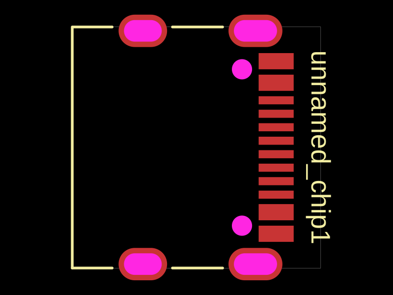 More from this authorAnasSarkiz/testDefines a PCB layout with a JST PH 2-pin connector labeled "J1".
 Similar packageimrishabh18/rp2040-motor-controllerAn RP2040-based NEMA17 stepper-motor controller with USB-C programming and PD motor-power negotiation, DRV8825 dual H-bridge drive, current/temperature telemetry, protected power filtering, status RGB LED, buzzer alarm, and optional magnetic encoder.
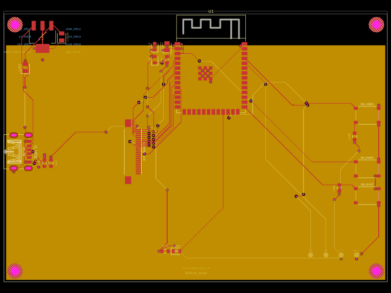 Discover something newShiboSoftwareDev/muse-reterminal-e1001-replacementA four-layer ESP32-S3 e-paper carrier board with USB-C power, AMS1117 3.3V regulation, 24-pin FFC interface, reset/boot and user buttons, status LED, decoupling passives, test points, mounting holes, and ground/power planes.