AnasSarkiz/NEMA14_RP2040
A NEMA motor assembly concept with a controller board, four proposed M3 screws and spacers, motor lead splices, and a JST 4-pin connector harness.
- Version
- 1.13.0
- License
- ISC
- Stars
- 0
scripts/find-reviewed-escapes.py
"""Construction only: route local TOP escapes against native pads and protected copper.
Ripped ordinary copper is recorded and must be rerouted and independently checked.
"""
import json,sys,heapq,math
import numpy as np
from PIL import Image,ImageDraw
from shapely.geometry import Point,LineString,box
import verify_supplier_connectivity as g
j=g.j;H=.025;LO=-17.5;N=1401
xy=lambda x,y:(round((x-LO)/H),round((y-LO)/H))
world=lambda p:(LO+p[0]*H,LO+p[1]*H)
thermal_sites=[]
for ref in ['U_MCU','U_DRV','U_PD']:
 c=next(c for c in g.comp.values() if g.src[c['source_component_id']]==ref);pad=next(e for e in j if e['type']=='pcb_smtpad' and e.get('pcb_component_id')==c['pcb_component_id'] and e.get('width',0)>1 and e.get('height',0)>1);off=json.loads((g.ROOT/'src/thermal-via-offsets.json').read_text())[ref];thermal_sites.append((pad['x']+off['x'],pad['y']+off['y']))
fixed=('usb_','oscillator_','reviewed_local_','review_escape_','reviewed_phase_inner1_')
allow_power_nets={a.split('=',1)[1] for a in sys.argv if a.startswith('--allow-power-net=')}
assert allow_power_nets<={'V3V3'}, 'Only the documented 3.3 V branch repair is supported'
def protected(e):
 if '--protect-signals' in sys.argv:return True
 if g.nets.get(g.key(e)) in {a.split('=',1)[1] for a in sys.argv if a.startswith('--protect-net=')}:return True
 if '--protect-power' in sys.argv and g.nets.get(g.key(e)) not in allow_power_nets and g.nets.get(g.key(e)) in {'PD_VBUS','DATA_VBUS','PD_VDD','LOGIC_IN','V3V3','V1V1','VREF','VCP','VREG','BUCK_SW','BUCK_BST','CP1','CP2','A_PLUS','A_MINUS','B_PLUS','B_MINUS','SENSE1','SENSE2'}:return True
 if e['type']=='pcb_via':return e['pcb_via_id'].startswith(fixed) or (g.nets.get(g.key(e))=='GND' and (e['pcb_via_id'].startswith('thermal') or any(math.dist((e['x'],e['y']),q)<.001 for q in thermal_sites))) or g.nets.get(g.key(e)) in ['USB_DP','USB_DM','MCU_DP','MCU_DM','XIN','XOUT','XTAL_OUT','QSPI_SCLK','QSPI_SD0','QSPI_SD1','QSPI_SD2','QSPI_SD3','QSPI_SS','RUN','SWCLK','SWDIO']
 return e['pcb_trace_id'].startswith(fixed) or g.nets.get(g.key(e)) in ['USB_DP','USB_DM','MCU_DP','MCU_DM','XIN','XOUT','XTAL_OUT','QSPI_SCLK','QSPI_SD0','QSPI_SD1','QSPI_SD2','QSPI_SD3','QSPI_SS','RUN','SWCLK','SWDIO']
def segments(e):
 if e['type']=='pcb_via':return [(layer,Point(e['x'],e['y']).buffer(e['outer_diameter']/2))]
 return [(a['layer'],LineString([(a['x'],a['y']),(b['x'],b['y'])]).buffer(max(a['width'],b['width'])/2)) for a,b in zip(e['route'],e['route'][1:]) if a['route_type']==b['route_type']=='wire' and a['layer']==b['layer']]
input_rows=json.load(open(sys.argv[1]))
if '--replace-group' in sys.argv:
 ids={identifier for row in input_rows for identifier in ['reviewed_local_'+row['ref']+'_'+row['role'],'reviewed_local_'+row['ref']+'_'+row['role']+'_via']}
 j[:]=[e for e in j if e.get(e['type']+'_id') not in ids]
for row in input_rows:
 ref,role=row['ref'],row['role'];uid='reviewed_local_'+ref+'_'+role
 p=next(p for p in g.ports.values() if g.src[g.sp[p['source_port_id']]['source_component_id']]==ref and g.sp[p['source_port_id']]['name']==role)
 layer=p.get('layers',['top'])[0];k=g.sp[p['source_port_id']]['subcircuit_connectivity_map_key'];name=g.nets[k];width=row.get('width',.3 if name in ['PD_VBUS','A_PLUS','A_MINUS','B_PLUS','B_MINUS','SENSE1','SENSE2','V3V3'] else .16)
 j[:]=[e for e in j if e.get(e['type']+'_id') not in [uid,uid+'_via'] and e['type']!='pcb_copper_pour']
 ims=[Image.new('L',(N,N)) for _ in range(2)];ds=[ImageDraw.Draw(im) for im in ims]
 def draw(idx,s,margin):
  s=s.buffer(margin,quad_segs=12)
  for q in list(s.geoms) if hasattr(s,'geoms') else [s]:
   if q.geom_type=='Polygon':ds[idx].polygon([xy(x,y) for x,y in q.exterior.coords],fill=1)
 for e in j:
  typ=e['type'];same=g.key(e)==k
  if typ in ['pcb_smtpad','pcb_plated_hole']:
   shape=g.geometry(e)
   if not same:
    draw(1,shape,.378)
    if layer in e.get('layers',[e.get('layer','top')]):draw(0,shape,width/2+.154)
   elif typ=='pcb_smtpad':draw(1,shape,.228)
  elif typ=='pcb_via' and same:
   draw(1,Point(e['x'],e['y']).buffer(e['hole_diameter']/2),.35)
  elif typ in ['pcb_trace','pcb_via'] and not same and protected(e):
   for l,shape in segments(e):
    draw(1,shape,.378)
    if l==layer:draw(0,shape,width/2+.18)
  elif typ=='pcb_keepout':
   c=e['center'];r=e['radius'];shape=Point(c['x'],c['y']).buffer(r,quad_segs=128);draw(0,shape,width/2+.15);draw(1,shape,.375)
  elif typ=='pcb_hole':
   shape=Point(e['x'],e['y']).buffer(e['hole_diameter']/2);draw(0,shape,width/2+.2);draw(1,shape,.35)
 for core in json.loads((g.ROOT/'artifacts/engineering-fixes/usb-routing-plan.json').read_text())['cores']:
  shape=LineString(core['centerline']).buffer(json.loads((g.ROOT/'src/layer-routing-policy.json').read_text()).get('USB_construction_reference_buffer_mm',.95))
  # Ground stitching has no foreign-net antipad in the reference plane.
  # Its real clearance to both USB tracks remains enforced above.
  if name!='GND':
   draw(1,shape,.425)
   if layer==core['reference_layer']:draw(0,shape,width/2+.154)
 for points in row.get('future_corridors',[]):
  shape=LineString(points).buffer(.08);draw(0,shape,width/2+.154);draw(1,shape,.378)
 for idx,r in [(0,.35+width/2),(1,.575)]:
  b=math.ceil(r/H);ds[idx].rectangle([0,0,N-1,b],fill=1);ds[idx].rectangle([0,N-1-b,N-1,N-1],fill=1);ds[idx].rectangle([0,0,b,N-1],fill=1);ds[idx].rectangle([N-1-b,0,N-1,N-1],fill=1)
 wire,via=[np.asarray(im,dtype=bool) for im in ims]
 start=xy(p['x'],p['y']);best={start:0};heap=[(0,start)];prev={};end=None;expanded=0
 radius=row.get('radius',5)
 reachable=np.load(row['reachable_sites']) if row.get('reachable_sites') else None
 if reachable is not None:assert reachable.shape==(N,N)
 while heap:
  cost,q=heapq.heappop(heap)
  if cost!=best[q]:continue
  x,y=world(q)
  if abs(x-p['x'])>radius or abs(y-p['y'])>radius:continue
  desired=row.get('desired_site')
  goal_ok=(desired is None or math.dist([x,y],desired)<.026) and (reachable is None or bool(reachable[q[1],q[0]]))
  if goal_ok and not via[q[1],q[0]] and not wire[q[1],q[0]]:end=q;break
  expanded+=1
  for dx,dy in [(1,0),(-1,0),(0,1),(0,-1),(1,1),(1,-1),(-1,1),(-1,-1)]:
   nx,ny=q[0]+dx,q[1]+dy
   if not(0<=nx<N and 0<=ny<N) or wire[ny,nx]:continue
   if dx and dy and (wire[q[1],nx] or wire[ny,q[0]]):continue
   a=(nx,ny);nc=cost+(2**.5 if dx and dy else 1)
   if nc<best.get(a,float('inf')):best[a]=nc;prev[a]=q;heapq.heappush(heap,(nc,a))
 if end is None:raise RuntimeError(f'No native-pad escape for {ref}:{role}, expanded {expanded}')
 path=[end]
 while path[-1]!=start:path.append(prev[path[-1]])
 path.reverse();slim=[path[0]]
 for i in range(1,len(path)-1):
  a,b,c=path[i-1:i+2]
  if (b[0]-a[0],b[1]-a[1])!=(c[0]-b[0],c[1]-b[1]):slim.append(b)
 slim.append(end);pts=[world(q) for q in slim];pts[0]=[p['x'],p['y']];site=pts[-1];wiregeom=LineString(pts).buffer(width/2);viageom=Point(site).buffer(.225);ripped=[]
 for e in list(j):
  if e['type'] not in ['pcb_trace','pcb_via'] or g.key(e)==k:continue
  if any(shape.distance(viageom)<.153 or l==layer and shape.distance(wiregeom)<.153 for l,shape in segments(e)):
   assert not protected(e),(ref,role,'protected collision',e[e['type']+'_id'])
   j.remove(e);ripped.append({'id':e[e['type']+'_id'],'type':e['type'],'net':g.nets[g.key(e)]})
 n=next(e for e in j if e['type']=='source_net' and e['name']==name);s=next(e for e in j if e['type']=='source_trace' and e.get('subcircuit_connectivity_map_key')==k and p['source_port_id'] in e.get('connected_source_port_ids',[]));attrs=dict(source_net_id=n['source_net_id'],source_trace_id=s['source_trace_id'],subcircuit_connectivity_map_key=k,subcircuit_id='subcircuit_source_group_0')
 route=[dict(route_type='wire',x=x,y=y,layer=layer,width=width) for x,y in pts];route[0]['start_pcb_port_id']=p['pcb_port_id']
 j.append(dict(type='pcb_trace',pcb_trace_id=uid,route=route,pcb_port_ids=[p['pcb_port_id']],**attrs));j.append(dict(type='pcb_via',pcb_via_id=uid+'_via',x=site[0],y=site[1],outer_diameter=.45,hole_diameter=.3,layers=['top','inner1','inner2','bottom'],from_layer='top',to_layer='bottom',tented_on_top=True,tented_on_bottom=True,**attrs))
 print(json.dumps(dict(ref=ref,role=role,net=name,points=pts,ripped=ripped)),flush=True)
 g.path.write_text(json.dumps(j,indent=2)+'\n')
Related Packages
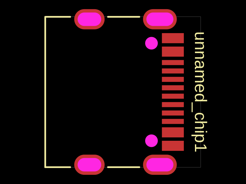 More from this authorAnasSarkiz/testDefines a PCB layout with a JST PH 2-pin connector labeled "J1".
 Similar packageimrishabh18/rp2040-motor-controllerAn RP2040-based NEMA17 stepper-motor controller with USB-C programming and PD motor-power negotiation, DRV8825 dual H-bridge drive, current/temperature telemetry, protected power filtering, status RGB LED, buzzer alarm, and optional magnetic encoder.
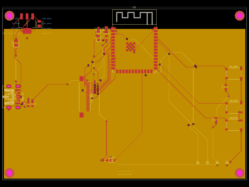 Discover something newShiboSoftwareDev/muse-reterminal-e1001-replacementA four-layer ESP32-S3 e-paper carrier board with USB-C power, AMS1117 3.3V regulation, 24-pin FFC interface, reset/boot and user buttons, status LED, decoupling passives, test points, mounting holes, and ground/power planes.