AnasSarkiz/NEMA14_RP2040
A NEMA stepper motor assembly concept with a controller board, proposed M3 screws and spacers, four motor leads with insulated splices, and a JST 4-pin connector harness.
- Version
- 1.12.2
- License
- ISC
- Stars
- 0
scripts/export-supplier-router.py
"""Export exact supplier land patterns, including polygons/slots, for checked routing."""
import json,math,pathlib,sys
from shapely.geometry import Polygon,box,Point
from shapely.affinity import rotate
ROOT=pathlib.Path(__file__).resolve().parents[1]
j=json.loads((ROOT/'artifacts/final-source.circuit.json').read_text());assert not any(e['type'].endswith('_error') for e in j),'Resolve source placement/connection errors before routing'
q=lambda s:json.dumps(str(s));um=lambda v:f'{v*1000:.4f}'
board=next(e for e in j if e['type']=='pcb_board');layer_names=['top','bottom'] if board['num_layers']==2 else ['top','inner2','bottom'];layer_map={'top':'F.Cu','inner2':'In2.Cu','bottom':'B.Cu'}
ports={e['pcb_port_id']:e for e in j if e['type']=='pcb_port'};sp={e['source_port_id']:e for e in j if e['type']=='source_port'};src={e['source_component_id']:e for e in j if e['type']=='source_component'}
nets={e['subcircuit_connectivity_map_key']:e['name'] for e in j if e['type']=='source_net'};netids={e['name']:e['source_net_id'] for e in j if e['type']=='source_net'}
for p in sp.values():
 key=p.get('subcircuit_connectivity_map_key')
 if key and key not in nets:nets[key]='DIRECT_'+key.rsplit('_',1)[-1]
shapes=[];images=[];placements=[];pinmap={};netpins={};pads=[e for e in j if e['type'] in ['pcb_smtpad','pcb_plated_hole']];count=0;thermal=[]
for c in [e for e in j if e['type']=='pcb_component']:
 cid=c['pcb_component_id'];cx,cy=c['center']['x'],c['center']['y'];pins=[]
 for pad in [e for e in pads if e['pcb_component_id']==cid]:
  count+=1;pid=pad.get('pcb_port_id');port=ports.get(pid,{});source=sp.get(port.get('source_port_id'),{});key=source.get('subcircuit_connectivity_map_key');net=nets.get(key,'NC_'+str(count));pin='p'+str(count);stack=[pad['layer']] if pad['type']=='pcb_smtpad' else layer_names
  if pad.get('shape')=='polygon':
   g=Polygon([(p['x'],p['y']) for p in pad['points']]).buffer(0);x,y=port['x'],port['y'];coords=[(vx-x,vy-y) for vx,vy in g.exterior.coords]
   desc=[f'(shape (polygon {layer_map[l]} 0 '+' '.join(um(v) for p in coords for v in p)+'))' for l in stack]
  else:
   x,y=pad['x'],pad['y'];w=pad.get('width',pad.get('outer_width',pad.get('outer_diameter',pad.get('radius',0)*2)));h=pad.get('height',pad.get('outer_height',pad.get('outer_diameter',pad.get('radius',0)*2)))
   if abs(pad.get('ccw_rotation',0)%180-90)<.01:w,h=h,w
   if pad.get('shape')=='circle':desc=[f'(shape (circle {layer_map[l]} {um(w)}))' for l in stack]
   elif pad.get('shape')=='pill':
    dx,dy=((w-h)/2,0) if w>=h else (0,(h-w)/2);desc=[f'(shape (path {layer_map[l]} {um(min(w,h))} {um(-dx)} {um(-dy)} {um(dx)} {um(dy)}))' for l in stack]
   else:desc=[f'(shape (rect {layer_map[l]} {um(-w/2)} {um(-h/2)} {um(w/2)} {um(h/2)}))' for l in stack]
  pname='supplier_pad_'+str(count);shapes.append(f'(padstack {q(pname)} '+' '.join(desc)+' (attach off))');pins.append(f'(pin {q(pname)} {q(pin)} {um(x-cx)} {um(y-cy)})');netpins.setdefault(net,[]).append(cid+'-'+pin);pinmap[cid+'-'+pin]={'pcb_port_id':pid,'net':net,'key':key}
  if src[c['source_component_id']]['name'] in ['U_MCU','U_PD','U_DRV'] and source.get('name') in ['GND','EP','PAD'] and pad.get('width',0)>1 and pad.get('height',0)>1:thermal.append({'x':x,'y':y,'net':'GND','component':src[c['source_component_id']]['name']})
 images.append(f'(image {q(cid)} '+' '.join(pins)+')');placements.append(f'(component {q(cid)} (place {q(cid)} {um(cx)} {um(cy)} front 0))')
keep=[]
for i,e in enumerate(j):
 if e['type']=='pcb_hole':
  for l in layer_names:keep.append(f'(keepout {q("hole"+str(i)+l)} (circle {layer_map[l]} {um(e["hole_diameter"]+.2)} {um(e["x"])} {um(e["y"])}))')
 if e['type']=='pcb_keepout':
  x,y=e['center']['x'],e['center']['y']
  if e['shape']=='circle':
   for l in layer_names:keep.append(f'(keepout {q("keep"+str(i)+l)} (rect {layer_map[l]} {um(x-e["radius"])} {um(y-e["radius"])} {um(x+e["radius"])} {um(y+e["radius"])}))')
   continue
  w,h=e['width'],e['height']
  for l in layer_names:keep.append(f'(keepout {q("keep"+str(i)+l)} (rect {layer_map[l]} {um(x-w/2)} {um(y-h/2)} {um(x+w/2)} {um(y+h/2)}))')
# Ground pad geometry and net identities remain in the native source/map.
# Autoroute signals; ground is completed with actual plane geometry and
# stitching, then independently checked for every physical ground pad.
wide=['PD_VBUS','A_PLUS','A_MINUS','B_PLUS','B_MINUS','SENSE1','SENSE2','V3V3','LOGIC_IN','BUCK_SW','BUZZER_SINK'];signal=[n for n in netpins if n not in wide];wide=[n for n in wide if n!='PD_VBUS'];classes=f'(class "signals" '+' '.join(q(n) for n in signal)+' (circuit (use_via "via400")) (rule (width 160) (clearance 150)))';classes+=f'(class "motor_power" '+' '.join(q(n) for n in wide)+' (circuit (use_via "via500")) (rule (width 300) (clearance 150)))'
classes+='(class "pd_power" "PD_VBUS" (circuit (use_via "via500")) (rule (width 550) (clearance 150)))'
via='(padstack "via500" '+' '.join(f'(shape (circle {layer_map[l]} 500))' for l in layer_names)+' (attach off))'
text='(pcb nema14_supplier (parser (string_quote ") (space_in_quoted_tokens on)) (resolution um 10) (unit um)'
text+='(structure '+' '.join(f'(layer {layer_map[l]} (type signal) (property (index {i})))' for i,l in enumerate(layer_names))+' (boundary (path pcb 0 -17200 -17200 17200 -17200 17200 17200 -17200 17200 -17200 -17200)) (via "via500" "via400") (rule (width 160) (clearance 150)) '+' '.join(keep)+')'
text+='(placement '+' '.join(placements)+') (library '+' '.join(images+shapes+[via]+[f'(padstack "via400" '+ ' '.join(f'(shape (circle {layer_map[l]} 400))' for l in layer_names)+' (attach off))'])+') (network '+' '.join(f'(net {q(n)} (pins '+' '.join(p for p in (pp if n!='GND' else []))+'))' for n,pp in netpins.items())+' '+classes+')'
wiring=[f'(via "via500" {um(v["x"])} {um(v["y"])} (net "GND") (type fix))' for v in thermal]
seed_file=ROOT/'artifacts/same-side-routing-seeds.json'
if seed_file.exists():
 seeds=json.loads(seed_file.read_text())
 for via_seed in seeds['vias']:
  if any(math.hypot(via_seed['x']-v['x'],via_seed['y']-v['y'])<.01 for v in thermal):continue
  assert (via_seed['outer_diameter'],via_seed['hole_diameter']) in [(0.5,0.25),(0.4,0.2)]
  via_name='via500' if via_seed['outer_diameter']==.5 else 'via400'
  net=nets[via_seed['subcircuit_connectivity_map_key']]
  wiring.append(f'(via {q(via_name)} {um(via_seed["x"])} {um(via_seed["y"])} (net {q(net)}) (type fix))')
 for trace in seeds['traces']:
  net=nets[trace['subcircuit_connectivity_map_key']]
  for a,b in zip(trace['route'],trace['route'][1:]):
   if a['route_type']!=b['route_type'] or a['route_type']!='wire' or a['layer']!=b['layer']:continue
   if math.hypot(a['x']-b['x'],a['y']-b['y'])<1e-8:continue
   assert a['layer'] in layer_names
   wiring.append(f'(wire (path {layer_map[a["layer"]]} {um(max(a["width"],b["width"]))} {um(a["x"])} {um(a["y"])} {um(b["x"])} {um(b["y"])}) (net {q(net)}) (type fix))')
text+='(wiring '+' '.join(wiring)+'))\n'
(ROOT/'artifacts/supplier-input.dsn').write_text(text);(ROOT/'artifacts/supplier-map.json').write_text(json.dumps({'pinmap':pinmap,'thermalVias':thermal,'netids':netids,'netkeys':{v:k for k,v in nets.items()}},indent=2)+'\n');(ROOT/'artifacts/supplier-unrouted.circuit.json').write_text(json.dumps(j,indent=2)+'\n')
print(count,'exact physical pads exported; ',len(netpins),'routing groups;',len(thermal),'grounded exposed-pad vias')
Related Packages
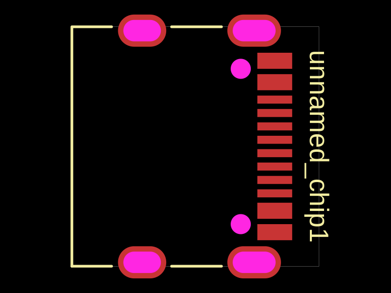 More from this authorAnasSarkiz/testDefines a PCB layout with a JST PH 2-pin connector labeled "J1".
 Similar packageimrishabh18/rp2040-motor-controllerAn RP2040-based NEMA17 stepper-motor controller with USB-C programming and PD motor-power negotiation, DRV8825 dual H-bridge drive, current/temperature telemetry, protected power filtering, status RGB LED, buzzer alarm, and optional magnetic encoder.
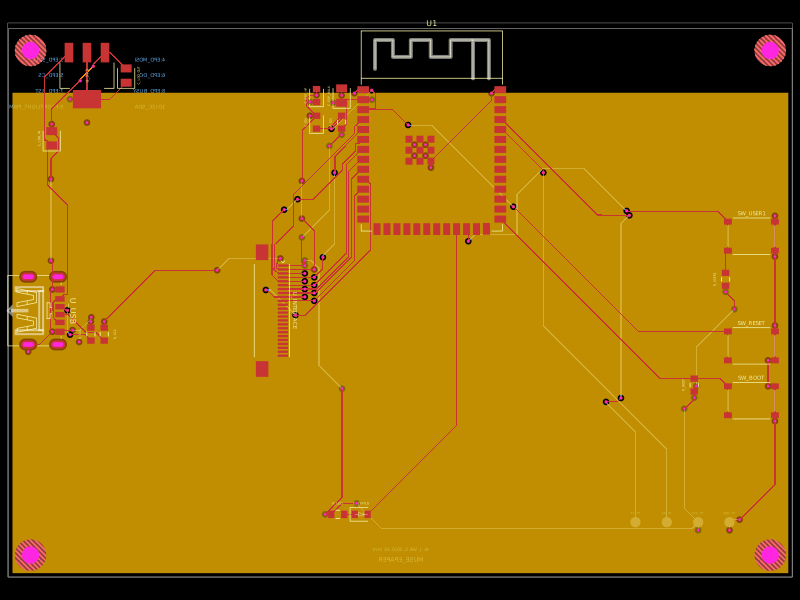 Discover something newShiboSoftwareDev/muse-reterminal-e1001-replacementA four-layer ESP32-S3 e-paper carrier board with USB-C power, AMS1117 3.3V regulation, 24-pin FFC interface, reset/boot and user buttons, status LED, decoupling passives, test points, mounting holes, and ground/power planes.