AnasSarkiz/NEMA14_RP2040
A NEMA stepper motor assembly concept with a controller board, proposed M3 screws and spacers, four motor leads with insulated splices, and a JST 4-pin connector harness.
- Version
- 1.12.2
- License
- ISC
- Stars
- 0
scripts/escape-ground-to-plane.py
"""Finish physically disconnected nets on exact supplier geometry.

The conservative routing grid is only a construction aid. Native DRC and the
independent physical/CAM checks are required afterward.
"""
import json, math, heapq, sys
import numpy as np
from PIL import Image,ImageDraw
from scipy.ndimage import distance_transform_edt
from shapely.ops import unary_union
import verify_supplier_connectivity as g

j=g.j;ROOT=g.ROOT;STEP=.025;LOW=-17.5;N=1401
layers=['top','bottom'] if next(e for e in j if e['type']=='pcb_board')['num_layers']==2 else ['top','inner2','bottom']
nets={e['subcircuit_connectivity_map_key']:e for e in j if e['type']=='source_net'}
traces={e['subcircuit_connectivity_map_key']:e['source_trace_id'] for e in j if e['type']=='source_trace'}
for k,name in g.nets.items():
 if k not in nets:nets[k]={'name':name,'source_net_id':None}
xy=lambda x,y:(round((x-LOW)/STEP),round((y-LOW)/STEP))
world=lambda q:(LOW+q[0]*STEP,LOW+q[1]*STEP)
def blocked(net,via=False):
    draw_layers=['top','inner1','inner2','bottom'] if via and next(e for e in j if e['type']=='pcb_board')['num_layers']==4 else layers
    images=[Image.new('L',(N,N)) for _ in draw_layers];ds=[ImageDraw.Draw(im) for im in images]
    margin=max(.15+current_via_diameter/2+.003,.20+current_via_hole/2+.003) if via else .15+current_width/2+.003
    def add(ls,geom):
        p=geom.buffer(margin,quad_segs=16)
        pieces=list(p.geoms) if hasattr(p,'geoms') else [p]
        for l in ls:
            if l not in draw_layers:continue
            d=ds[draw_layers.index(l)]
            for piece in pieces:
                if piece.geom_type=='Polygon':d.polygon([xy(x,y) for x,y in piece.exterior.coords],fill=1)
    for e in j:
        typ=e['type']
        if typ in ['pcb_smtpad','pcb_plated_hole']:
            if g.key(e)==net and not via:continue
            add(e.get('layers',[e.get('layer','top')]),g.geometry(e))
        elif typ=='pcb_via':
            if g.key(e)==net and not via:continue
            add(draw_layers,g.Point(e['x'],e['y']).buffer(e['outer_diameter']/2))
        elif typ=='pcb_trace' and g.key(e)!=net:
            for a,b in zip(e['route'],e['route'][1:]):
                if a['route_type']==b['route_type']=='wire' and a['layer']==b['layer']:
                    add([a['layer']],g.LineString([(a['x'],a['y']),(b['x'],b['y'])]).buffer(max(a['width'],b['width'])/2))
        elif typ=='pcb_keepout':
            # Use the actual circular mounting envelope.
            c=e['center'];r=e['radius'];add(e['layers'],g.Point(c['x'],c['y']).buffer(r,quad_segs=128))
        elif typ=='pcb_hole':add(draw_layers,g.Point(e['x'],e['y']).buffer(e['hole_diameter']/2+.1))
    b=math.ceil((.35+(current_via_diameter/2 if via else current_width/2))/STEP)
    for d in ds:
        d.rectangle([0,0,N-1,b],fill=1);d.rectangle([0,N-1-b,N-1,N-1],fill=1)
        d.rectangle([0,0,b,N-1],fill=1);d.rectangle([N-1-b,0,N-1,N-1],fill=1)
    return [np.asarray(im,dtype=np.bool_) for im in images]

# Ground returns may join the reserved plane at any legal through-via site.
# No track is placed on inner1; the native all-layer via joins the actual plane.
from collections import deque
from shapely.geometry import Polygon
net=next(k for k,n in g.nets.items() if n=='GND');source_net=nets[net]['source_net_id'];current_width=.16
board=next(e for e in j if e['type']=='pcb_board');current_via_diameter=board['min_via_pad_diameter'];current_via_hole=board['min_via_hole_diameter'];receipts=[]
for attempt in range(80):
 elems,roots=g.groups(net);islands={}
 for e,r in zip(elems,roots):
  if e.get('pcb_port_id'):islands.setdefault(r,[]).append(e)
 main=max(islands,key=lambda r:len(islands[r]))
 if '--force' in sys.argv:
  requested=json.loads((ROOT/'artifacts/reference-feedback/forced-ground-ports.json').read_text())['ports']
  for pad in [e for e in j if e['type'] in ['pcb_smtpad','pcb_plated_hole'] and e.get('pcb_port_id') in requested]:
   if not any(t['type']=='pcb_trace' and t.get('pcb_trace_id','').startswith('feedback_ground_escape_'+pad['pcb_port_id']) for t in j):islands[('force',pad['pcb_port_id'])]=[pad]
 if len(islands)<2:break
 planes=[]
 for e,r in zip(elems,roots):
  if r==main and e['type']=='pcb_copper_pour' and e['layer']=='inner1':
   b=e['brep_shape'];pts=lambda q:[(v['x'],v['y']) for v in q['vertices']];planes.append(Polygon(pts(b['outer_ring']),[pts(q) for q in b.get('inner_rings',[])]))
 if not planes:raise RuntimeError('A reserved connected inner1 ground plane is required')
 plane=unary_union(planes).buffer(-.01);wire=blocked(net);vm=blocked(net,True);via_clear=np.logical_not(np.logical_or.reduce(vm));found=None
 for r in sorted((r for r in islands if r!=main),key=lambda r:len(islands[r])):
  for pad in islands[r]:
   p=g.ports[pad['pcb_port_id']];l=layers.index(pad.get('layer','top'));start=xy(p['x'],p['y'])
   if wire[l][start[1],start[0]]:continue
   queue=deque([start]);previous={start:None};end=None
   while queue and len(previous)<160000:
    q=queue.popleft();x,y=q
    if via_clear[y,x] and plane.covers(g.Point(*world(q))):end=q;break
    for dx,dy in [(1,0),(-1,0),(0,1),(0,-1),(1,1),(1,-1),(-1,1),(-1,-1)]:
     nx,ny=x+dx,y+dy;nq=(nx,ny)
     if not(0<=nx<N and 0<=ny<N) or nq in previous or wire[l][ny,nx]:continue
     if dx and dy and (wire[l][y,nx] or wire[l][ny,x]):continue
     previous[nq]=q;queue.append(nq)
   if end is None:continue
   path=[end]
   while previous[path[-1]] is not None:path.append(previous[path[-1]])
   path.reverse();slim=[path[0]]
   for a,b,c in zip(path,path[1:],path[2:]):
    if (b[0]-a[0],b[1]-a[1])!=(c[0]-b[0],c[1]-b[1]):slim.append(b)
   slim.append(path[-1]);route=[{'route_type':'wire','x':world(q)[0],'y':world(q)[1],'layer':layers[l],'width':.16} for q in slim];route[0].update(x=p['x'],y=p['y'],start_pcb_port_id=pad['pcb_port_id']);x,y=world(end)
   sid=next(t['source_trace_id'] for t in j if t['type']=='source_trace' and t.get('subcircuit_connectivity_map_key')==net and p['source_port_id'] in t.get('connected_source_port_ids',[]));uid='feedback_ground_escape_'+pad['pcb_port_id']
   while any(e.get('pcb_trace_id')==uid for e in j):uid+='_next'
   j.append({'type':'pcb_trace','pcb_trace_id':uid,'route':route,'source_net_id':source_net,'source_trace_id':sid,'subcircuit_connectivity_map_key':net,'subcircuit_id':'subcircuit_source_group_0','pcb_port_ids':[pad['pcb_port_id']]})
   j.append({'type':'pcb_via','pcb_via_id':uid+'_via','x':x,'y':y,'outer_diameter':current_via_diameter,'hole_diameter':current_via_hole,'layers':['top','inner1','inner2','bottom'],'from_layer':'top','to_layer':'bottom','source_net_id':source_net,'source_trace_id':sid,'subcircuit_connectivity_map_key':net,'subcircuit_id':'subcircuit_source_group_0','tented_on_top':True,'tented_on_bottom':True})
   found={'port':pad['pcb_port_id'],'via_xy_mm':[x,y],'trace':uid,'layer':layers[l]};receipts.append(found);print(found,flush=True);g.path.write_text(json.dumps(j,indent=2)+'\n');break
  if found:break
 if not found:break
print('Ground roots remaining:',len(islands));(ROOT/'artifacts/reference-feedback/ground-escapes.json').write_text(json.dumps({'escapes':receipts,'remaining_ground_roots':len(islands),'reserved_plane':'inner1','no_additional_via_in_pad':True},indent=2)+'\n')
Related Packages
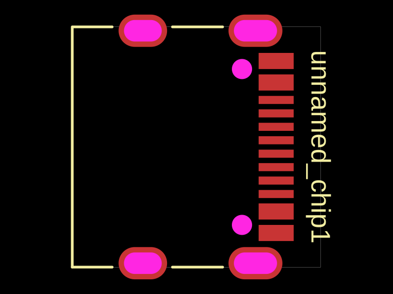 More from this authorAnasSarkiz/testDefines a PCB layout with a JST PH 2-pin connector labeled "J1".
 Similar packageimrishabh18/rp2040-motor-controllerAn RP2040-based NEMA17 stepper-motor controller with USB-C programming and PD motor-power negotiation, DRV8825 dual H-bridge drive, current/temperature telemetry, protected power filtering, status RGB LED, buzzer alarm, and optional magnetic encoder.
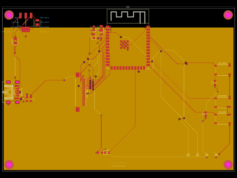 Discover something newShiboSoftwareDev/muse-reterminal-e1001-replacementA four-layer ESP32-S3 e-paper carrier board with USB-C power, AMS1117 3.3V regulation, 24-pin FFC interface, reset/boot and user buttons, status LED, decoupling passives, test points, mounting holes, and ground/power planes.