AnasSarkiz/NEMA14_RP2040
A NEMA motor assembly concept with a controller board, four proposed M3 screws and spacers, motor lead splices, and a JST 4-pin connector harness.
- Version
- 1.13.0
- License
- ISC
- Stars
- 0
scripts/check-usb-reference.py
"""Independent checks of actual coupled copper and its adjacent grounded reference.

Geometry evidence only: impedance requires the fabricator's verified stackup,
while USB operation requires firmware and bench testing.
"""
import hashlib,json,math
from shapely.ops import unary_union
import verify_supplier_connectivity as g
j=g.j;plan=json.loads((g.ROOT/'artifacts/engineering-fixes/usb-routing-plan.json').read_text());nets={e['name']:e['subcircuit_connectivity_map_key'] for e in j if e['type']=='source_net'};errors=[];rows=[]
def pour(e):
 b=e['brep_shape'];pts=lambda ring:[(p['x'],p['y']) for p in ring['vertices']];return g.Polygon(pts(b['outer_ring']),[pts(r) for r in b.get('inner_rings',[])])
for core in plan['cores']:
 lines=[];tracks=[];ref=unary_union([pour(e) for e in j if e['type']=='pcb_copper_pour' and e['layer']==core['reference_layer'] and g.key(e)==nets['GND']]);transitions=unary_union([g.Point(e['x'],e['y']).buffer(e['outer_diameter']/2+.21) for e in j if e['type']=='pcb_via' and g.key(e) in [nets[t['net']] for t in core['tracks']]])
 for t in core['tracks']:
  e=next((e for e in j if e.get('pcb_trace_id')==t['trace_id']),None)
  if e is None:errors.append('Missing actual core '+t['trace_id']);continue
  points=[(p['x'],p['y']) for p in e['route']];line=g.LineString(points);lines.append(line)
  if points!=[tuple(p) for p in t['points']] or any(p.get('layer')!=core['layer'] or p.get('width')!=.25 for p in e['route']):errors.append('Core differs from construction receipt '+t['trace_id'])
  es,rs=g.groups(nets[t['net']]);roots={r for q,r in zip(es,rs) if q.get('pcb_trace_id')==t['trace_id']};lands={r for q,r in zip(es,rs) if q.get('pcb_port_id')}
  if not roots or not roots<=lands:errors.append('Unconnected core '+t['trace_id'])
  points=[line.interpolate(s) for s in [min(i*.025,line.length) for i in range(math.ceil(line.length/.025)+1)]];screen=[p for p in points if not transitions.covers(p)];missing=[p for p in screen if not ref.buffer(.000002).covers(p)];screen_line=line.difference(transitions);unsupported_line=screen_line.difference(ref.buffer(.000002));fraction=1-unsupported_line.length/max(screen_line.length,1e-12)
  if not screen or fraction<1-.00001:errors.append('Insufficient adjacent GND reference '+t['trace_id']+' '+str(round(fraction,4)))
  screened_copper=line.buffer(.125).difference(transitions)
  unsupported_copper=screened_copper.difference(ref.buffer(.000002))
  copper_coverage=1-unsupported_copper.area/max(screened_copper.area,1e-12)
  if unsupported_copper.area>1e-6:errors.append('Insufficient full-width adjacent GND reference '+t['trace_id']+' '+str(round(copper_coverage,6)))
  tracks.append({'full_width_ground_reference_coverage_fraction':copper_coverage,'unsupported_reference_copper_area_mm2':unsupported_copper.area,'net':t['net'],'trace_id':t['trace_id'],'actual_length_mm':line.length,'screened_reference_samples':len(screen),'local_USB_via_antipad_samples':len(points)-len(screen),'ground_reference_coverage_fraction':fraction,'exact_screened_reference_length_mm':screen_line.length,'exact_unsupported_reference_length_mm':unsupported_line.length,'unsupported_samples_mm':[[p.x,p.y] for p in missing]})
 if len(lines)==2:
  gap=lines[0].distance(lines[1])-.25;skew=abs(lines[0].length-lines[1].length)
  if gap<.15-.000002:errors.append('Coupled clearance below 0.15 mm '+core['name'])
  if skew>.5:errors.append('Core length skew above 0.5 mm '+core['name'])
 else:gap=skew=None
 rows.append({'core':core['name'],'layer':core['layer'],'reference_layer':core['reference_layer'],'actual_minimum_pair_clearance_mm':gap,'core_length_difference_mm':skew,'tracks':tracks})
for e in j:
 if e['type']=='pcb_trace' and g.key(e) in [nets[n] for n in ['USB_DP','USB_DM','MCU_DP','MCU_DM'] if n in nets] and any(p.get('layer') in ['inner1','inner2'] for p in e['route']):errors.append('USB routed on inner signal layer '+e['pcb_trace_id'])
report={'passed':not errors,'board_sha256':hashlib.sha256(g.path.read_bytes()).hexdigest(),'cores':rows,'nominal_core_width_mm':.25,'nominal_core_gap_mm':.16,'local_terminal_fanouts_width_mm':.16,'reference_coverage_method':'Exact geometric intersection of every screened track centerline with grounded adjacent-layer copper; 0.025 mm samples retained for diagnosis','reference_transition_exceptions':'Only actual same-pair via antipads, pad radius plus 0.21 mm; no blanket endpoint exclusion','controlled_impedance_verified':False,'fabricator_stackup_approved':False,'USB_hardware_operation_verified':False,'errors':errors};(g.ROOT/'artifacts/engineering-fixes/usb-verification.json').write_text(json.dumps(report,indent=2)+'\n');print(json.dumps(report,indent=2));raise SystemExit(bool(errors))
Related Packages
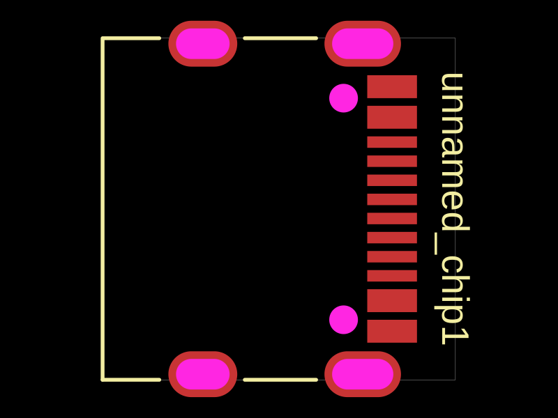 More from this authorAnasSarkiz/testDefines a PCB layout with a JST PH 2-pin connector labeled "J1".
 Similar packageimrishabh18/rp2040-motor-controllerAn RP2040-based NEMA17 stepper-motor controller with USB-C programming and PD motor-power negotiation, DRV8825 dual H-bridge drive, current/temperature telemetry, protected power filtering, status RGB LED, buzzer alarm, and optional magnetic encoder.
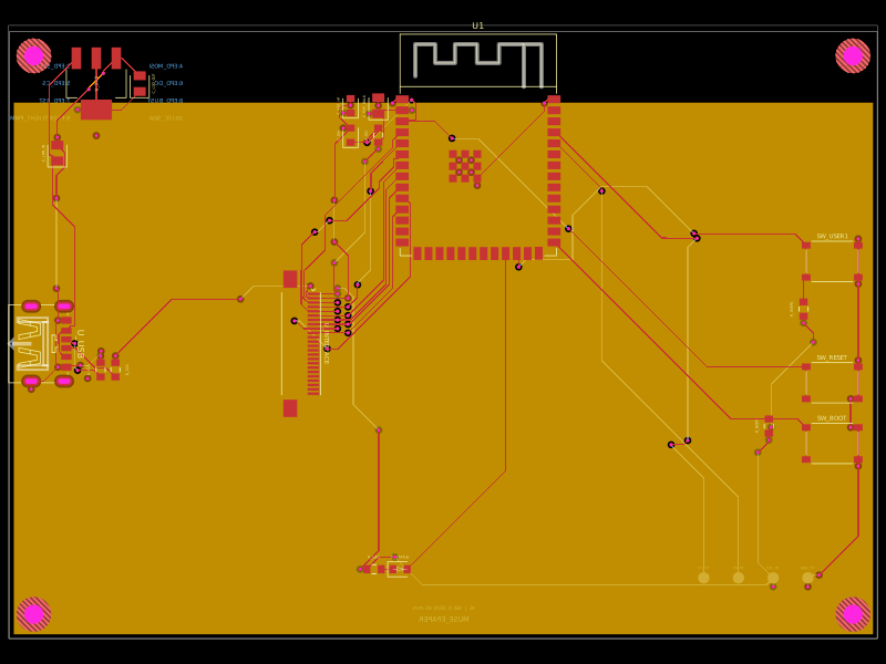 Discover something newShiboSoftwareDev/muse-reterminal-e1001-replacementA four-layer ESP32-S3 e-paper carrier board with USB-C power, AMS1117 3.3V regulation, 24-pin FFC interface, reset/boot and user buttons, status LED, decoupling passives, test points, mounting holes, and ground/power planes.